JAJSGI0D November 2018 – January 2021 TPS63802
PRODUCTION DATA
- 1 特長
- 2 アプリケーション
- 3 概要
- 4 Revision History
- 5 概要 (続き)
- 6 Device Comparison Table
- 7 Pin Configuration and Functions
- 8 Specifications
-
9 Detailed Description
- 9.1 Overview
- 9.2 Functional Block Diagram
- 9.3
Feature Description
- 9.3.1 Control Loop Description
- 9.3.2 Precise Device Enable: Threshold- or Delayed Enable
- 9.3.3 Mode Selection (PFM/PWM)
- 9.3.4 Undervoltage Lockout (UVLO)
- 9.3.5 Soft Start
- 9.3.6 Adjustable Output Voltage
- 9.3.7 Overtemperature Protection - Thermal Shutdown
- 9.3.8 Input Overvoltage - Reverse-Boost Protection (IVP)
- 9.3.9 Output Overvoltage Protection (OVP)
- 9.3.10 Power-Good Indicator
- 9.4 Device Functional Modes
- 10Application and Implementation
- 11Power Supply Recommendations
- 12Layout
- 13Device and Documentation Support
- 14Mechanical, Packaging, and Orderable Information
9.3.5 Soft Start
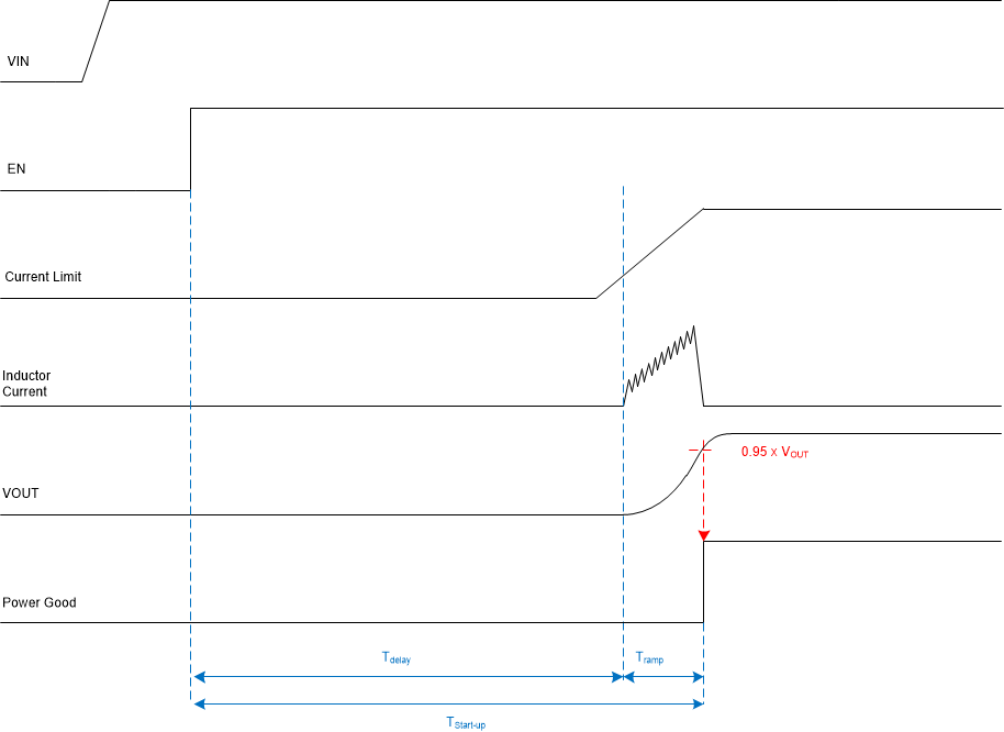
To minimize inrush current and output voltage overshoot during start-up, the device features a controlled soft start-up. After the device is enabled, the device starts all internal reference and control circuits within the enable delay time, Tdelay. After that, the maximum switch current limit rises monotonically from 0 mA to the current limit. The loop stops switching once VO is reached. This allows a quick output voltage ramp for small capacitors at the output. The bigger the output capacitor, the longer it takes to settle Vo. A potential load during start-up will lengthen the duration of the output voltage ramp as well. The gradual ramp of the current limit allows a small inrush current for no-load conditions, as well as the possibility to start into high loads at start-up.
The converter can start-up into pre-biased loads by a forced operation in PFM during the soft-start until the first switching cycle request from the output voltage control loop.
 Figure 9-4 Device Start-up Scheme