SLVSCF4A December 2014 – July 2016 TPS650830
PRODUCTION DATA.
- 1 Device Overview
- 2 Revision History
- 3 Device Options
- 4 Pin Configuration and Functions
- 5 Specifications
-
6 Detailed Description
- 6.1 Overview
- 6.2 Functional Block Diagram
- 6.3
Feature Description
- 6.3.1 Voltage Regulator Assignment and Powergood Comparator Logic Assignment (External Voltage Regulator or Load Switch) for Skylake and Kabylake Platform
- 6.3.2 Generic Powergood Window Comparator with Open-Drain Output
- 6.3.3 Powergood Window Comparator
- 6.3.4 3.3-V LDO and 3V3SW Load Switch
- 6.3.5 5-V LDO and 5VSW Load Switch
- 6.3.6 RTC Selector and 3.1-V LDO
- 6.3.7 Power Path Comparators
- 6.3.8 UVLO Comparators
- 6.3.9 Temperature Comparator
- 6.3.10 Low Power Mode (LPM) / Connected Standby / Instant Go of VRs
- 6.3.11 Enable and Powergood of VRs
- 6.3.12 VR4 VDDQ and LDO1 VTT Enabling
- 6.3.13
Converters
- 6.3.13.1 Power Save Mode
- 6.3.13.2 Voltage Regulator Startup
- 6.3.13.3 Powergood, Power Fault, and Emergency Power Shutdown
- 6.3.13.4 Current Limit
- 6.3.13.5 Output Discharge Feature
- 6.3.13.6 Output Voltage Control
- 6.3.13.7 Converter Low Power Mode Operation
- 6.3.13.8 Controller Low Power Mode Operation
- 6.3.13.9 Controller Internal Ramp Comparator
- 6.3.13.10 Undervoltage Lockout
- 6.3.14 Coincell Selector
- 6.4 Device Functional Modes
- 6.5 Programming
- 6.6
Register Map
- 6.6.1
Registers
- 6.6.1.1 VENDORID Register (address = 0x00) [reset = 00100010]
- 6.6.1.2 REVID Register (address = 0x01) [reset = 00000000]
- 6.6.1.3 IRQLVL1 Register (address = 0x02) [reset = 00000000]
- 6.6.1.4 PWRSRCINT Register (address = 0x04) [reset = 00000000]
- 6.6.1.5 PMUINT Register (address = 0x05) [reset = 00000000]
- 6.6.1.6 RESETIRQ1 Register (address = 0x08) [reset = 00000000]
- 6.6.1.7 RESETIRQ2 Register (address = 0x09) [reset = 00000000]
- 6.6.1.8 MPMUINT Register (address = 0x0B) [reset = 00010100]
- 6.6.1.9 MPWRSRCINT Register (address = 0x0C) [reset = 01111000]
- 6.6.1.10 RESETIRQ1MASK Register (address = 0x11) [reset = 00110000]
- 6.6.1.11 RESETIRQ2MASK Register (address = 0x12) [reset = 00000010]
- 6.6.1.12 IRQLVL1msK Register (address = 0x13) [reset = 10100101]
- 6.6.1.13 PBCONFIG Register (address = 0x14) [reset = 00011111]
- 6.6.1.14 PBSTATUS Register (address = 0x15) [reset = 00000000]
- 6.6.1.15 PWRSTAT1 Register (address = 0x16) [reset = 00000000]
- 6.6.1.16 PWRSTAT2 Register (address = 0x17) [reset = 00000000]
- 6.6.1.17 PGMASK1 Register (address = 0x18) [reset = 00000000]
- 6.6.1.18 PGMASK2 Register (address = 0x19) [reset = 00000000]
- 6.6.1.19 VCCIOCNT Register (address = 0x30) [reset = 00001010]
- 6.6.1.20 V5ADS3CNT Register (address = 0x31) [reset = 00101010]
- 6.6.1.21 V33ADSWCNT Register (address = 0x32) [reset = 00101010]
- 6.6.1.22 V33APCHCNT Register (address = 0x33) [reset = 00001010]
- 6.6.1.23 V18ACNT Register (address = 0x34) [reset = 00101010]
- 6.6.1.24 V18U25UCNT Register (address = 0x35) [reset = 00001010]
- 6.6.1.25 V1P2UCNT Register (address = 0x36) [reset = 00111010]
- 6.6.1.26 V100ACNT Register (address = 0x37) [reset = 00011010]
- 6.6.1.27 V085ACNT Register (address = 0x38) [reset = 00101010]
- 6.6.1.28 VRMODECTRL Register (address = 0x3B) [reset = 00111111]
- 6.6.1.29 DISCHCNT1 Register (address = 0x3C) [reset = 00000000]
- 6.6.1.30 DISCHCNT2 Register (address = 0x3D) [reset = 00000000]
- 6.6.1.31 DISCHCNT3 Register (address = 0x3E) [reset = 00000000]
- 6.6.1.32 DISCHCNT4 Register (address = 0x3F) [reset = 00000000]
- 6.6.1.33 PWRGDCNT1 Register (address = 0x40) [reset = 01011111 ]
- 6.6.1.34 VREN Register (address = 0x41) [reset = 00000000]
- 6.6.1.35 REGLOCK Register (address = 0x42) [reset = 00000000]
- 6.6.1.36 VRENPINMASK Register (address = 0x43) [reset = 00000000]
- 6.6.1.37 RSTCTRL Register (address = 0x48) [reset = 00011100]
- 6.6.1.38 SDWNCTRL Register (address = 0x49) [reset = 00000000]
- 6.6.1.39 VDLMTCRT Register (address = 0x51) [reset = 00000101]
- 6.6.1.40 ACOKDBDM Register (address = 0x69) [reset = 00001111]
- 6.6.1.41 LOWBATTDET Register (address = 0x6A) [reset = 11111000]
- 6.6.1.42 SPWRSRCINT Register (address = 0x6F) [reset = 00000000]
- 6.6.1.43 CLKCTRL1 Register (address = 0xD0) [reset = 00000000]
- 6.6.1.44 COMPA_REF Register (address = 0xDD) [reset = 00000000]
- 6.6.1.45 COMPB_REF Register (address = 0xDE) [reset = 00000000]
- 6.6.1.46 COMPC_REF Register (address = 0xDF) [reset = 00000000]
- 6.6.1.47 COMPD_REF Register (address = 0xE0) [reset = 00000000]
- 6.6.1.48 COMPE_REF Register (address = 0xE1) [reset = 00000000]
- 6.6.1.49 COMPF_REF Register (address = 0xE2) [reset = 00000000]
- 6.6.1.50 COMPG_REF Register (address = 0xE3) [reset = 00000000]
- 6.6.1.51 COMPH_REF Register (address = 0xE4) [reset = 00000000]
- 6.6.1.52 PWFAULT_MASK1 Register (address = 0xE5) [reset = 00000000]
- 6.6.1.53 PWFAULT_MASK2 Register (address = 0xE6) [reset = 00000000]
- 6.6.1.54 PGOOD_STAT1 Register (address = 0xE7) [reset = 00000000]
- 6.6.1.55 PGOOD_STAT2 Register (address = 0xE8) [reset = 00000000]
- 6.6.1.56 MISC_BITS Register (address = 0xE9) [reset = 00010000]
- 6.6.1.57 STDBY_CTRL Register (address = 0xEA) [reset = 11111110]
- 6.6.1.58 TEMPCRIT Register (address = 0xEB) [reset = 00000000]
- 6.6.1.59 TEMPHOT Register (address = 0xEC) [reset = 00000000]
- 6.6.1.60 VREN_PIN_OVR Register (address = 0xEE) [reset = 00000000]
- 6.6.1
Registers
-
7 Application and Implementation
- 7.1 Application Information
- 7.2
Typical Application
- 7.2.1 Design Requirements
- 7.2.2 Detailed Design Procedure
- 7.2.3 Application Performance Curves
- 7.2.4 Specific Application - TPS650830 Powering the Intel SkyLake and Kabylake Platform Volume Configuration
- 7.3 System Example
- 7.4 Do's and Don'ts
- 8 Power Supply Recommendations
- 9 Layout
- 10Device and Documentation Support
- 11Mechanical, Packaging, and Orderable Information
パッケージ・オプション
メカニカル・データ(パッケージ|ピン)
サーマルパッド・メカニカル・データ
発注情報
9 Layout
9.1 Layout Guidelines
For all switching power supplies, the layout is an important step in the design, especially at high peak currents and high switching frequencies. If the layout is not carefully done, the regulator could show stability problems as well as EMI problems. Therefore, use wide and short traces for the main current path and for the power ground tracks. The input capacitor, output capacitor, and the inductor should be placed as close as possible to the IC. Use a common ground node for power ground and a different one for control ground to minimize the effects of ground noise. Connect these ground nodes at any place close to one of the ground pins of the IC.
There are 2 packages available for the TPS65083x, the ZAJ and ZCG. The ZAJ is a 7-mm x 7-mm BGA with 0.5-mm ball pitch. The ZCG is a 9-mm x 9-mm BGA with 0.5-mm ball pitch but, some of the inner balls have been removed for easier routing. Both packages preform relatively the same and the decision between which package is best for the application depends on the space constraints and routing technology used.
9.1.1 Fanout for ZAJ using Type 4 Routing
This small 7-mm x 7-mm package utilizes the Type 4 routing technique to decrease system board area as much as possible. This Type 4 routing has vias in pad, blind and buried vias, and minimum trace width / spacing of 4 mils.
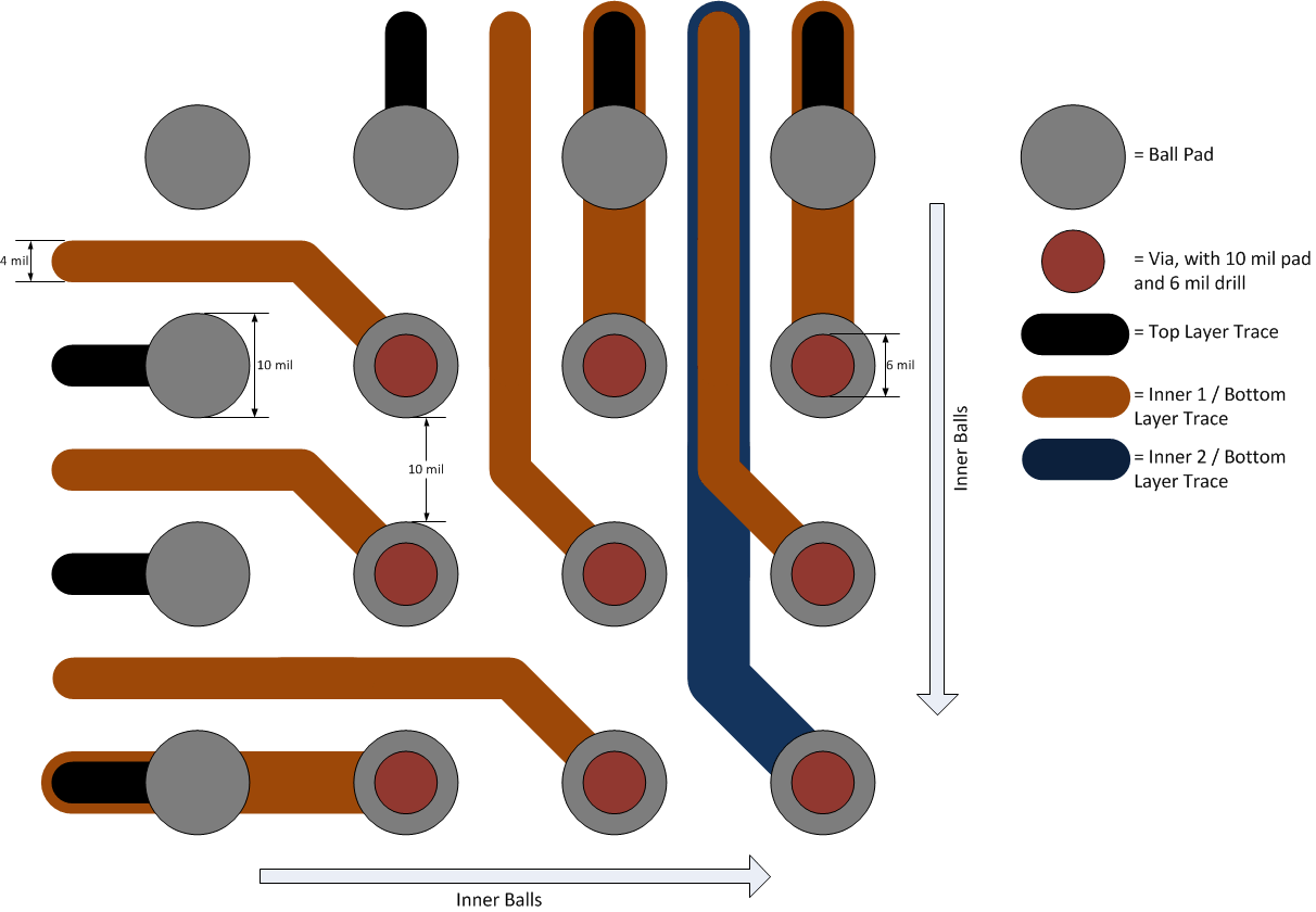 Figure 9-1 Fanout for ZAJ Package Using Type 4 Routing
9.1.2 Fanout for ZCG using Type 3 Routing
The ZCG has some of the inner balls removed to essentially create a 0.1-mm ball pitch for the inner balls of the package. This feature allows for Type 3 routing of the board. This Type 3 routing has no vias in pad, no blind and buried vias, and minimum trace width / spacing of 4 mils.
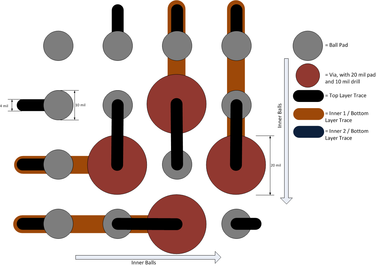 Figure 9-2 Fanout for ZCG Package using Type 3 Routing
9.1.3 Layout Checklist
- All inductors, input/output caps and FETs for the converters and controller should be on the same board layer as the IC.
- Place feedback connection points near the output capacitors and minimize the control feedback loop as much as possible to achieve the best regulation performance.
- Bootstrap capacitors must be place close to the IC from the SWVRx to VBSTVRx pins.
- DRVLVRx signals must be routed on the same layer as the IC and the FETs and minimize the length and parasitic inductance of the trace as much as possible.
- Each converter and controller should have their own separate ground and each ground should connect to the common ground separately. The input capacitors, output capacitors, and FET grounds for each VRx converter and controller must be connected to the ground plane for the respective VRx rail. Since, the PGNDs for each rail are not connect to each other or AGND, it is required to use the PGNDVRx pins for the input and output capacitors for each VRx rail. This ground plane should connect in one place to the common ground close to the input and output capacitor ground pads. See the figure below for a visual representation of the converter layout scheme.
- The internal reference regulators must have their input and output caps close to the IC pins.
- Route the FBVRxP and FBVRxN signals as a differential pair.
9.2 Layout Example
9.2.1 Controller Layout
The routing of the controllers is critical to the performance of the power supply. To reduce the risk of the controller effecting other sensitive circuits on the board, it is recommended to place all of the controller components on the same layer are the PMIC. In addition to component placement, the DRV, SW, and PGND signals should be routed on the same layer or as few of layers possible. It is recommended to place the FETs as close as possible to the PMIC but, it is imperative that the input capacitors are placed with minimal distance from the VIN and PGND pads of the FETs. The feedback signals should be routed differentially to the furthest output capacitor, which should be placed close to the load. Be sure to not route the feedback or any analog sensitive signals under the inductor, next to the SW node, or between the CIN and the FETs due to the high frequency switching from the edges.
If the FETs of the controller are to be place far away from the PMIC the layout of the DRV, SW and PGND signals becomes extremely critical. The loop inductance of the the traces must be minimized as much as possible. In-order to do this, pair the DRVH and SW traces together and pair the DRVL and PGND traces together. PGND is best routed as a plane. To reduce the loop inductance of the DRVL, DRVL trace should be routed one layer above the PGND. Generally, the SW, DRVL and DRVH traces should be 20 mils or larger assuming the PGND is a plane underneath the DRVL trace.
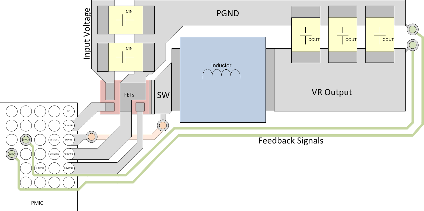 Figure 9-3 Controller Layout Diagram
9.2.2 ZAJ Package
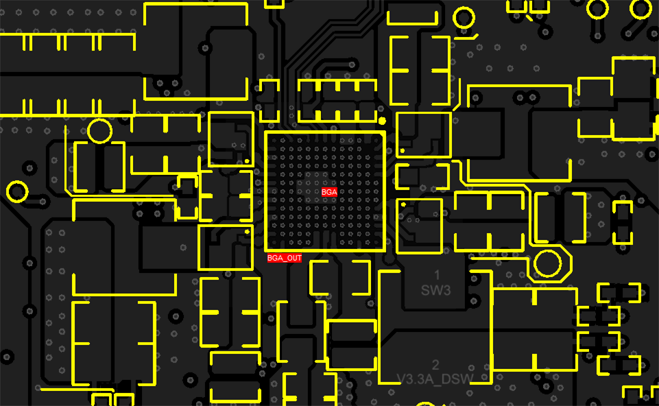 Figure 9-4 Top Layer ZAJ Layout
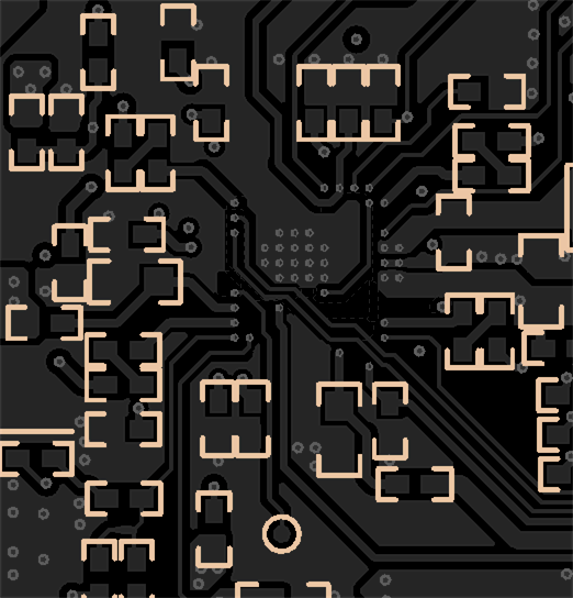 Figure 9-5 Bottom Layer ZAJ Layout
9.2.3 ZCG Package
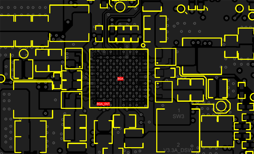 Figure 9-6 Top Layer ZCG Layout
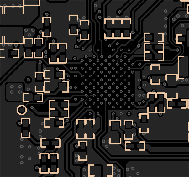 Figure 9-7 Bottom Layer ZCG Layout
9.3 Thermal Considerations
Implementation of integrated circuits in low-profile and fine-pitch surface-mount packages typically requires special attention to power dissipation. Many system-dependent issues such as thermal coupling, airflow, added heat sinks and convection surfaces, and the presence of other heat-generating components affect the power-dissipation limits of a given component.
Three basic approaches for enhancing thermal performance are listed below.
- Improving the power dissipation capability of the PCB design
- Improving the thermal coupling of the component to the PCB by soldering the PowerPAD™
- Introducing airflow in the system
For more details on how to use the thermal parameters in the dissipation ratings table please check the Thermal Characteristics Application Note (SZZA017) and the IC Package Thermal Metrics Application Note (SPRA953).