SLVS849C July 2008 – September 2017 TPS65100-Q1
PRODUCTION DATA.
- 1 Features
- 2 Applications
- 3 Description
- 4 Revision History
- 5 Pin Configuration and Functions
- 6 Specifications
- 7 Detailed Description
-
8 Application and Implementation
- 8.1 Application Information
- 8.2
Typical Applications
- 8.2.1
Supply for a Typical Approximately 7-inch Display
- 8.2.1.1 Design Requirements
- 8.2.1.2
Detailed Design Procedure
- 8.2.1.2.1
Boost Converter Design Procedure
- 8.2.1.2.1.1 Inductor Selection
- 8.2.1.2.1.2 Output Capacitor Selection
- 8.2.1.2.1.3 Input Capacitor Selection
- 8.2.1.2.1.4 Rectifier Diode Selection
- 8.2.1.2.1.5 Converter Loop Design and Stability
- 8.2.1.2.1.6 Design Procedure Quick Steps
- 8.2.1.2.1.7 Setting the Output Voltage and Selecting the Feedforward Capacitor
- 8.2.1.2.2 Negative Charge Pump
- 8.2.1.2.3 Positive Charge Pump
- 8.2.1.2.4 VCOM Buffer
- 8.2.1.2.5 Linear Regulator Controller
- 8.2.1.2.1
Boost Converter Design Procedure
- 8.2.1.3 Application Curves
- 8.2.2 Supply for a Typical Approximately 8-inch Display
- 8.2.1
Supply for a Typical Approximately 7-inch Display
- 9 Power Supply Recommendations
- 10Layout
- 11Device and Documentation Support
- 12Mechanical, Packaging, and Orderable Information
パッケージ・オプション
メカニカル・データ(パッケージ|ピン)
- PWP|24
サーマルパッド・メカニカル・データ
- PWP|24
発注情報
6 Specifications
6.1 Absolute Maximum Ratings
over operating free-air temperature range (unless otherwise noted)(1)| MIN | MAX | UNIT | ||
|---|---|---|---|---|
| Voltage range(2) | VIN | –0.3 | 6 | V |
| SUP | –0.3 | 15.5 | ||
| EN, MODE, ENR | –0.3 | VI + 0.3 | ||
| Voltage | VCOMIN | 14 | V | |
| Voltage(2) | SW | 20 | V | |
| Continuous power dissipation | See Thermal Information | |||
| Operating junction temperature range | –40 | 150 | °C | |
| Lead temperature (soldering, 10 seconds) | 260 | °C | ||
| Storage temperature, Tstg | –65 | 150 | °C | |
(1) Stresses beyond those listed under Absolute Maximum Ratings may cause permanent damage to the device. These are stress ratings only, which do not imply functional operation of the device at these or any other conditions beyond those indicated under Recommended Operating Conditions. Exposure to absolute-maximum-rated conditions for extended periods may affect device reliability.
(2) Voltage values are with respect to network ground terminal.
6.2 ESD Ratings
| VALUE | UNIT | |||
|---|---|---|---|---|
| V(ESD) | Electrostatic discharge | Human-body model (HBM), per AEC Q100-002(1) | ±2000 | V |
| Charged-device model (CDM), per AEC Q100-011 | ±1000 | |||
| Machine model (MM) | ±100 | |||
(1) AEC Q100-002 indicates that HBM stressing shall be in accordance with the ANSI/ESDA/JEDEC JS-001 specification.
6.3 Recommended Operating Conditions
| MIN | NOM | MAX | UNIT | ||
|---|---|---|---|---|---|
| VI | Input voltage | 2.7 | 5.8 | V | |
| L | Inductor(1) | 4.7 | μH | ||
| TA | Operating free-air temperature | –40 | 125 | °C | |
(1) See Inductor Selection for further information.
6.4 Thermal Information
| THERMAL METRIC(1) | TPS65100-Q1 | UNIT | |
|---|---|---|---|
| PWP (TSSOP) | |||
| 24 PINS | |||
| RθJA | Junction-to-ambient thermal resistance | 37.2 | °C/W |
| RθJC(top) | Junction-to-case (top) thermal resistance | 19.5 | °C/W |
| RθJB | Junction-to-board thermal resistance | 16.7 | °C/W |
| ψJT | Junction-to-top characterization parameter | 0.4 | °C/W |
| ψJB | Junction-to-board characterization parameter | 16.6 | °C/W |
| RθJC(bot) | Junction-to-case (bottom) thermal resistance | 2.1 | °C/W |
(1) For more information about traditional and new thermal metrics, see the Semiconductor and IC Package Thermal Metrics application report, SPRA953.
6.5 Electrical Characteristics
VI = 3.3 V, EN = VIN, VO1 = 10 V, TJ = –40°C to 125°C, typical values are at TA = 25°C (unless otherwise noted)| PARAMETER | TEST CONDITIONS | MIN | TYP | MAX | UNIT | |
|---|---|---|---|---|---|---|
| SUPPLY CURRENT | ||||||
| IQ | Quiescent current into VIN | ENR = VCOMIN = GND, VO3 = 2 × VO1, Boost converter not switching |
0.7 | 0.9 | mA | |
| IQCharge | Charge pump quiescent current into SUP | VO1 = SUP = 10 V, VO3 = 2 × VO1 | 1.7 | 2.7 | mA | |
| VO1 = SUP = 10 V, VO3 = 3 × VO1 | 3.9 | 6 | ||||
| IQVCOM | VCOM quiescent current into SUP | ENR = GND, VO1 = SUP = 10 V | 750 | 1300 | μA | |
| IQEN | LDO controller quiescent current into VIN | ENR = VIN, EN = GND | 300 | 800 | μA | |
| ISD | Shutdown current into VIN | EN = ENR = GND | 1 | 10 | μA | |
| VUVLO | Undervoltage lockout threshold | VIN falling | 2.2 | 2.4 | V | |
| Thermal shutdown | Temperature rising | 160 | °C | |||
| LOGIC SIGNALS EN, ENR | ||||||
| VIH | High-level input voltage | 1.5 | V | |||
| VIL | Low-level input voltage | 0.4 | V | |||
| ILeak | Input leakage current | EN = GND or VIN | 0.01 | 0.1 | μA | |
| MAIN BOOST CONVERTER | ||||||
| VO1 | Output voltage range | 5 | 15 | V | ||
| VO1 - VI | Minimum input to output voltage difference |
1 | V | |||
| VREF | Reference voltage | 1.198 | 1.213 | 1.230 | V | |
| VFB | Feedback regulation voltage | 1.126 | 1.146 | 1.161 | V | |
| IFB | Feedback input bias current | 10 | 100 | nA | ||
| rDS(ON) | N-MOSFET on-resistance (Q1) | VO1 = 10 V, Isw = 500 mA | 195 | 325 | mΩ | |
| VO1 = 5 V, Isw = 500 mA | 285 | 455 | ||||
| ILIM | N-MOSFET switch current limit (Q1) | 1.6 | 2.3 | 2.7 | A | |
| rDS(ON) | P-MOSFET on-resistance (Q2) | VO1 = 10 V, Isw = 100 mA | 9 | 15 | Ω | |
| VO1 = 5 V, Isw = 100 mA | 14 | 22 | ||||
| IMAX | Maximum P-MOSFET peak switch current | 1 | A | |||
| ILeak | Switch leakage current | Vsw = 15 V | 1 | 10 | μA | |
| fSW | Oscillator frequency | 0°C ≤ TJ ≤ 125°C | 1.195 | 1.6 | 2.1 | MHz |
| –40°C ≤ TJ ≤ 125°C | 1.091 | 1.6 | 2.1 | |||
| Line regulation | 2.7 V ≤ VI ≤ 5.7 V, Iload = 100 mA | 0.012 | %/V | |||
| Load regulation | 0 mA ≤ IO ≤ 300 mA | 0.2 | %/A | |||
| NEGATIVE CHARGE PUMP VO2 | ||||||
| VO2 | Output voltage range | –2 | V | |||
| VREF | Reference voltage | 1.198 | 1.213 | 1.226 | V | |
| VFB | Feedback regulation voltage | –36 | 0 | 36 | mV | |
| IFB | Feedback input bias current | 10 | 100 | nA | ||
| rDS(ON) | Q8 P-channel switch rDS(ON) | IO = 20 mA | 4.3 | 8 | Ω | |
| Q9 N-channel switch rDS(ON) | 2.9 | 4.4 | ||||
| IO | Maximum output current | 20 | mA | |||
| Line regulation | 7 V ≤ VO1 ≤ 15 V, Iload = 10 mA, VO2 = –5 V | 0.09 | %/V | |||
| Load regulation | 1 mA ≤ IO ≤ 20 mA, VO2 = –5 V | 0.126 | %/mA | |||
| POSITIVE CHARGE PUMP VO3 | ||||||
| VO3 | Output voltage range | 30 | V | |||
| VREF | Reference voltage | 1.198 | 1.213 | 1.226 | V | |
| VFB | Feedback regulation voltage | 1.180 | 1.214 | 1.245 | V | |
| IFB | Feedback input bias current | 10 | 100 | nA | ||
| rDS(ON) | Q3 P-channel switch rDS(ON) | IO = 20 mA | 9.9 | 15.5 | Ω | |
| Q4 N-channel switch rDS(ON) | 1.1 | 1.8 | ||||
| Q5 P-channel switch rDS(ON) | 4.6 | 8.5 | ||||
| Q6 N-channel switch rDS(ON) | 1.2 | 2.2 | ||||
| VD | D1–D4 Shottky diode forward voltage | ID1–D4 = 40 mA | 610 | 800 | mV | |
| IO | Maximum output current | 20 | mA | |||
| Line regulation | 10 V ≤ VO1 ≤ 15 V, Iload = 10 mA, VO3 = 27 V | 0.56 | %/V | |||
| Load regulation | 1 mA ≤ IO ≤ 20 mA, VO3 = 27 V | 0.05 | %/mA | |||
| LINEAR REGULATOR CONTROLLER VO4 | ||||||
| VO4 | Output voltage | 4.5 V ≤ VI ≤ 5.5 V, 10 mA ≤ IO ≤ 500 mA | 3.2 | 3.3 | 3.4 | V |
| IBASE | Maximum base drive current | VI - VO4 - VBE ≥ 0.5 V (1) | 13.5 | 19 | mA | |
| VI - VO4 - VBE ≥ 0.75 V (1) | 20 | 27 | ||||
| Line regulation | 4.75 V ≤ VI ≤ 5.5 V, Iload = 500 mA | 0.186 | %/V | |||
| Load regulation | 1 mA ≤ IO ≤ 500 mA, VI = 5 V | 0.064 | %/A | |||
| Start up current | VO4 ≤ 0.8 V | 11 | 20 | 25 | mA | |
| VCOM BUFFER | ||||||
| VCM | Common mode input range | 2.25 | (VO1) - 2 | V | ||
| VOS | Input offset voltage | IO = 0 mA | –25 | 25 | mV | |
| DC Load regulation | IO = ±25 mA | –30 | 37 | mV | ||
| IO = ±50 mA | –45 | 55 | ||||
| IO = ±100 mA | –72 | 85 | ||||
| IO = ±150 mA | –97 | 110 | ||||
| IB | VCOMIN Input bias current | –300 | –30 | 300 | nA | |
| IPeak | Peak output current | VO1 = 15 V | 1.2 | A | ||
| VO1 = 10 V | 0.65 | A | ||||
| VO1 = 5 V | 0.15 | A | ||||
| FAULT PROTECTION THRESHOLDS | ||||||
| V(th, Vo1) | Shutdown threshold | VO1 Rising | –12 | –8.75% VO1 | –6 | V |
| V(th, Vo2) | VO2 Rising | –13 | –9% VO2 | –5 | V | |
| V(th, Vo3) | VO3 Rising | –11 | –8% VO3 | –5 | V | |
(1) With VI = supply voltage of the TPS65100-Q1, VO4 = output voltage of the regulator, VBE = basis emitter voltage of external transistor
6.6 Typical Characteristics
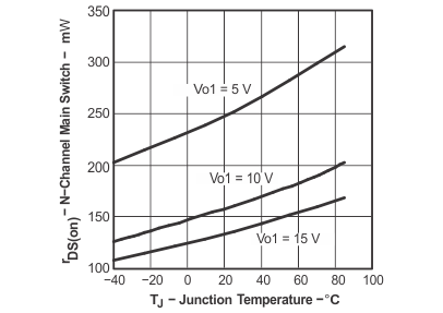
 Figure 1. rDS(ON) N-Channel Main Switch vs
Junction Temperature
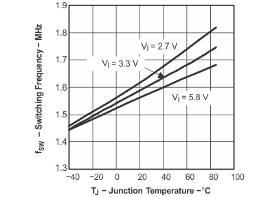
 Figure 2. Switching Frequency vs Junction Temperature