SLVSBB2E May 2012 – March 2017 TPS65131-Q1
PRODUCTION DATA.
- 1 Features
- 2 Applications
- 3 Description
- 4 Revision History
- 5 Pin Configuration and Functions
- 6 Specifications
- 7 Parameter Measurement Information
- 8 Detailed Description
-
9 Application and Implementation
- 9.1 Application Information
- 9.2
Typical Applications
- 9.2.1
TPS65131-Q1 With VPOS = 10.5 V, VNEG = -10 V
- 9.2.1.1 Design Requirements
- 9.2.1.2 Detailed Design Procedure
- 9.2.1.3 Analog Supply Input Filter
- 9.2.1.4 Thermal Information
- 9.2.1.5 Application Curves
- 9.2.2 TPS65131-Q1 With VPOS = 5.5 V, VNEG = -5 V
- 9.2.3 TPS65131-Q1 With VPOS = 15 V, VNEG = -15 V
- 9.2.1
TPS65131-Q1 With VPOS = 10.5 V, VNEG = -10 V
- 10Power Supply Recommendations
- 11Layout
- 12Device and Documentation Support
- 13Mechanical, Packaging, and Orderable Information
パッケージ・オプション
メカニカル・データ(パッケージ|ピン)
- RGE|24
サーマルパッド・メカニカル・データ
- RGE|24
発注情報
9 Application and Implementation
NOTE
Information in the following applications sections is not part of the TI component specification, and TI does not warrant its accuracy or completeness. TI’s customers are responsible for determining suitability of components for their purposes. Customers should validate and test their design implementation to confirm system functionality.
9.1 Application Information
The TPS656131-Q1 boost converter output voltage, VPOS, and the inverting converter output voltage, VNEG, require external components to set the required output voltages. The valid output voltage ranges are as shown in Recommended Operating Conditions). The passages below show typical application examples with different output voltage settings and guidance for external component choices.
9.2 Typical Applications
9.2.1 TPS65131-Q1 With VPOS = 10.5 V, VNEG = –10 V
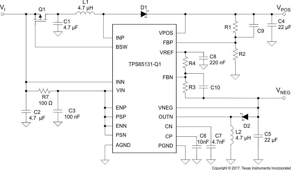 Figure 6. Typical Application Schematic With VPOS = 10.5 V, VNEG = –10 V
9.2.1.1 Design Requirements
This design example uses the following parameters:
Table 2. Design Parameters
| Design Parameter | Example Value | |||
|---|---|---|---|---|
| Input voltage range | 2.7 V to 5.5 V | |||
| Boost converter output voltage, VPOS | R1 = 1 MΩ R2 = 130 kΩ C9 = 6.8 pF |
10.5 V | ||
| Inverting converter output voltage, VNEG | R3 = 1 MΩ R4 = 121.2 kΩ C10 = 7.5 pF |
–10 V | ||
In this example, the converters operate with power-save mode both enabled and disabled (see Power-Save Mode).
9.2.1.2 Detailed Design Procedure
9.2.1.2.1 Programming the Output Voltage
9.2.1.2.1.1 Boost Converter
An external resistor divider adjusts the output voltage of the TPS65131-Q1 boost converter stage. Connect this divider to the FBP pin. The typical value of the voltage at the FBP pin is the reference voltage, which is 1.213 V. The maximum recommended output voltage at the boost converter is 15 V. To achieve appropriate accuracy, the current through the feedback divider should be about 100 times higher than the current into the FBP pin. Typical current into the FBP pin is 0.05 µA, and the voltage across R2 is 1.213 V. Based on those values, the recommended value for R2 should be lower than 200 kΩ in order to set the divider current at 5 µA or higher.
Calculate the value of resistor R1, as a function of the needed output voltage (VPOS), with Equation 1:

In this example, with R2 = 130 kΩ, choose R1 = 1 MΩ to set VPOS = 10.5 V.
9.2.1.2.1.2 Inverting Converter
An external resistor divider adjusts the output voltage of the TPS65131-Q1 inverting converter stage. Connect this divider to the FBN pin. Unlike the feedback divider at the boost converter, the reference point of the feedback divider is not GND, but Vref. So the typical value of the voltage at the FBN pin is 0 V. The minimum recommended output voltage at the inverting converter is –15 V. Feedback divider current considerations are similar to the considerations for the boost converter. For the same reasons, the feedback divider current should be in the range of 5 µA or higher. The voltage across R4 is 1.213 V. Based on those values, the recommended value for R4 should be lower than 200 kΩ in order to set the divider current at the required value.
Calculate the value of resistor R3, as a function of the needed output voltage (VNEG), with Equation 2:

In this example, with R4 = 121.2 kΩ kΩ, choose R3 = 1 MΩ to set VNEG = –10 V.
9.2.1.2.2 Inductor Selection
An inductive converter normally requires two main passive components to store energy during the conversion. Therefore, each converter requires an inductor and a storage capacitor. To select the right inductor, it is recommended to keep the possible peak inductor current below the current-limit threshold of the power switch in the chosen configuration. For example, the current-limit threshold of the switch for the boost converter and for the inverting converters is nominally 1950 mA. The highest peak current through the switches and the inductor depends on the output load (IPOS, INEG), the input voltage (VI), and the output voltages (VPOS, VNEG). Use Equation 3 to estimate the peak inductor current in the boost converter, I(L-P). Equation 4 shows the corresponding formula for the inverting converter, I(L-N).


The second parameter for choosing the inductor is the desired current ripple in the inductor. Normally, it is advisable to work with a ripple of less than 20% of the average inductor current. A smaller ripple reduces the losses in the inductor, as well as output voltage ripple and EMI. But in the same way, output voltage regulation gets slower, causing higher voltage changes during fast load changes. In addition, a larger inductor usually increases the total system cost. Keep those parameters in mind and calculate the possible inductor value with Equation 5 for the boost converter (L1) and Equation 6 for the inverting converter (L2).


The parameter f is the switching frequency. For the boost converter, ΔI(L-P) is the ripple current in the inductor, that is, 20% of I(L-P). Accordingly, for the inverting converter, ΔI(L-N) is the ripple current in the inductor, that is, 20% of I(L-N). VI is the input voltage, which is 3.3 V in this example. So, the calculated inductance value for the boost inductor is 5.1 µH and for the inverting converter inductor is 5.1 µH. With these calculated values and the calculated currents, it is possible to choose a suitable inductor.
In typical applications, the recommendation is to choose a 4.7-µH inductor. The device is optimized to work with inductance values between 3.3 µH and 6.8 µH. Nevertheless, operation with higher inductance values may be possible in some applications. Perform detailed stability analysis in this case. Be aware of the possibility that load transients and losses in the circuit can lead to higher currents than estimated in Equation 3 and Equation 4. Also, the losses caused by magnetic hysteresis and conductor resistance are a major parameter for total circuit efficiency.
The following table shows inductors from different suppliers used with the TPS65131-Q1 converter:
Table 3. List of Inductors
| VENDOR(1) | INDUCTOR SERIES |
|---|---|
| EPCOS | B8246284-G4 |
| Wurth Elektronik | 7447789XXX |
| 744031XXX | |
| TDK | VLF3010 |
| VLF4012 | |
| Cooper Electronics Technologies | SD12 |
9.2.1.2.3 Capacitor Selection
9.2.1.2.3.1 Input Capacitor
As a recommendation, choose an input capacitors of at least 4.7 µF for the input of the boost converter (INP) and accordingly for the input of the inverting converter (INN). This improves transient behavior of the regulators and EMI behavior of the total power-supply circuit. Choose a ceramic capacitor or a tantalum capacitor. For the use of a tantalum capcitor, an additonal, smaller ceramic capacitor (100 nF) in parallel is required. Place the input capacitor(s) close to the input pins.
9.2.1.2.3.2 Output Capacitors
One of the major parameters necessary to define the capacitance value of the output capacitor is the maximum allowed output voltage ripple of the converter. Two parameters, which are the capacitance and the equivalent series resitance (ESR), affect this ripple. It is possible to calculate the minimum capacitance needed for the defined ripple, supposing that the ESR is zero. Use Equation 7 for the boost-converter output capacitor (C4min) and Equation 8 for the inverting-converter output capacitor (C5min).


The parameter f is the switching frequency. ΔVPOS and ΔVNEG are the maximum allowed ripple voltages for each converter.
Choosing a ripple voltage in the range of 10 mV requires a minimum capacitance of 12 µF. The total ripple is larger due to the ESR of the output capacitor. Use Equation 9 for the boost converter and Equation 10 for the inverting converter to calculate this additional ripple component.


In this example, an additional ripple of 2 mV is the result of using a typical ceramic capacitor with an ESR in the 10-mΩ range. The total ripple is the sum of the ripple caused by the capacitance and the ripple caused by the ESR of the capacitor. In this example, the total ripple is 10 mV.
Load transients can create additional ripple. When the load current increases rapidly, the output capacitor must provide the additional current until the inductor current increases by the control loop which sets a higher on-time (duty cycle) of the main switch. The higher duty cycle results in longer inductor charging periods. The inductance itself also limits the rate of increase of the inductor current. When the load current decreases rapidly, the output capacitor must store the excess energy (stored in the inductor) until the regulator has decreased the inductor current by reducing the duty cycle. The recommendation is to use higher capacitance values, as the foregoing calculations show.
9.2.1.2.4 Rectifier Diode Selection
Both converters (the boost and inverting converter) require rectifier diodes, D1 and D2. As a recommendation, to reduce losses, use Schottky diodes. The forward current rating needed is equal to the maximum output current. Consider that the maximum currents, IPOSmax and INEGmax, might differ for VPOS and VNEG when choosing the diodes.
9.2.1.2.5 External P-MOSFET Selection
During shutdown, when connected to a power supply, a path from the power supply to the positive output conducts through the inductor and an external diode. Optionally, in oder to fully disconnect the positive output VPOS during shutdown, add an external p-MOSFET (Q1). The BSW pin controls the gate of the p-MOSFET. When choosing a proper p-MOSFET, the VGS and VGD voltage ratings must cover the input voltage range, the drain current rating must not be lower than the maximum input current flowing into the application, and conditions of the p-MOSFET operating area must fit.
If there is no intention to use an external p-MOSFET, leave the BSW pin floating.
9.2.1.2.6 Stabilizing the Control Loop
9.2.1.2.6.1 Feedforward Capacitors
As a recommendation, to speed up the control loop, place feedforward capacitors in the feedback divider, parallel to R1 (boost converter) and R3 (inverting converter). Equation 11 shows how to calculate the appropriate value for the boost converter, and Equation 12 for the inverting converter.


In this application example, C9 = 6.8 pF and C10 = 7.5 pF match the choices of R1 and R3.
To avoid coupling noise into the control loop from the feedforward capacitors, it is possible to place a series resistor to limit the bandwidth of the feedforward effect. Any value between 10 kΩ and 100 kΩ is suitable. The higher the resistance, the lower the noise coupled into the control loop system.
9.2.1.2.6.2 Compensation Capacitors
The device features completely internally compensated control loops for both converters. The internal feedforward system has built-in error correction which requires external capacitors. As a recommendation, use a 10-nF capacitor at the CP pin of the boost converter and a 4.7-nF capacitor at the CN pin of the inverting converter.
9.2.1.3 Analog Supply Input Filter
To ensure a noise free voltage supply of the IC, it is recommended to add an RC or LC filter between IIN and VIN pins.
9.2.1.3.1 RC-Filter
For most applications an RC filter can be used with a resistance value of 100 Ω minimum and capacitor value of 0.1 µF as in the application example Figure 6.
9.2.1.3.2 LC-Filter
For applications where input voltages VI with a fast rising edge (slew rate ≥ 275 mV/µs) are expected, it is recommended to replace the resistor R7 with a ferrite bead to minimize the delay between the signals on IIN and VIN. A ferrite bead with the lowest possible DCR and a proper current rating should be selected - BLM18KG101TN1 for example. A conservative approach for the current rating specification is to set it at 1.5 times or twice the maximum input current.
Table 4. List of Ferrite Beads
| VENDOR | FERRITE BEAD SERIES |
|---|---|
| Murata | BLMxKG |
9.2.1.4 Thermal Information
Implementation of integrated circuits in low-profile and fine-pitch surface-mount packages typically requires special attention to power dissipation. Many system-dependent issues, such as thermal coupling, airflow, added heatsinks and convection surfaces, and the presence of heat-generating components affect the power-dissipation limits of a given component.
Three basic approaches for enhancing thermal performance follow.
- Improving the power dissipation capability of the PCB design
- Improving the thermal coupling of the component to the PCB
- Introducing airflow to the system
The recommended device junction temperature range, TJ, is –40°C to 125°C. The thermal resistance of the 24-pin QFN, 4–mm × 4–mm package (RGE) is RθJA = 34.1°C/W. The recommended operating ambient temperature range for the device is TA = –40°C to 105°C. Use Equation 13 to calculate the maximum power dissipation, PDmax, as a function of TA. In this equation, use TJ = 125°C to operate the device within the recommended temperature range, use TJ = T(TS) to determine the absolute maximum threshold when the device might go into thermal shutdown. If the maximum ambient temperature of the application is lower, more heat dissipation is possible.
9.2.1.5 Application Curves
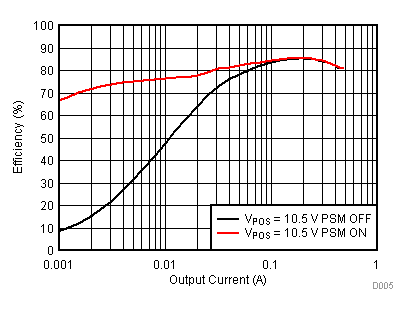
| VI = 3.3 V | VPOS = 10.5 V | Power-save mode on and off |
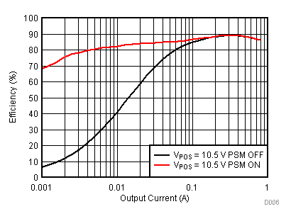
| VI = 5 V | VPOS = 10.5 V | Power-save mode on and off |
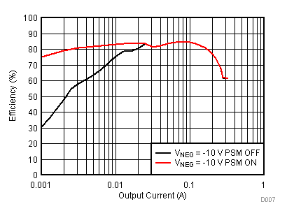
| VI = 3.3 V | VNEG = –10 V | Power-save mode on and off |
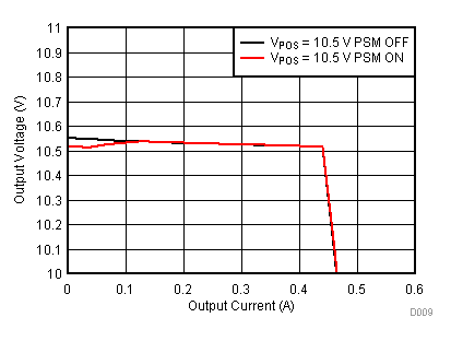
| VI = 3.3 V | VPOS = 10.5 V | Power-save mode on and off |
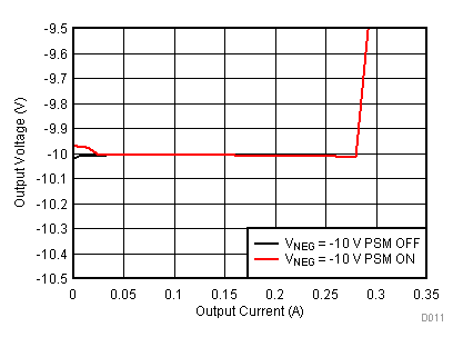
| VI = 3.3 V | VNEG = –10 V | Power-save mode on and off |
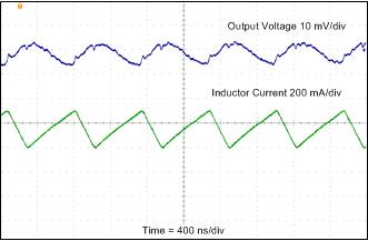
| VI = 3.3 V | VPOS = 10.5 V IPOS = 200 mA |
Power-save mode off |
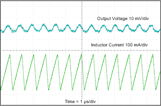
| VI = 3.3 V | VNEG = –10 V INEG = 200 mA |
Power-save mode off |
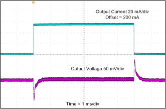
| VI = 3.3 V | VPOS = 10.5 V | |
| IPOS = 200 mA to 250 mA | ||
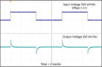
| VI = 3 V to 3.6 V | VPOS = 10.5 V | IPOS = 150 mA |
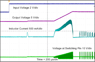
| VI = 3.3 V | VPOS = 10.5 V | IPOS = 46 mA |
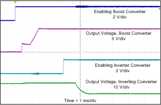
| VI = 3.3 V | VPOS = 10.5 V | VNEG = –10 V |
| IPOS = INEG= 160 mA |
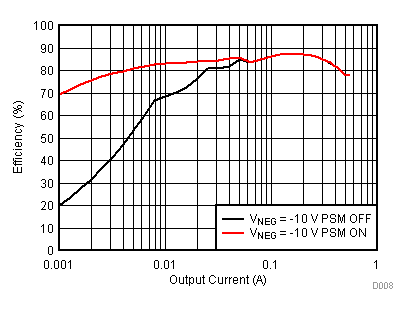
| VI = 5 V | VNEG = –10 V | Power-save mode on and off |
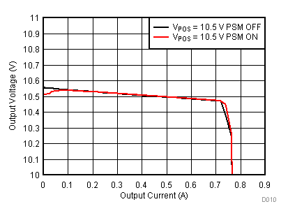
| VI = 5 V | VPOS = 10.5 V | Power-save mode on and off |
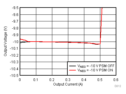
| VI = 5 V | VNEG = –10 V | Power-save mode on and off |
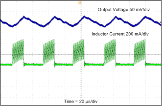
| VI = 3.3 V | VPOS = 10.5 V IPOS = 20 mA |
Power-save mode on |
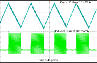
| VI = 3.3 V | VNEG = –10 V INEG = 20 mA |
Power-save mode on |
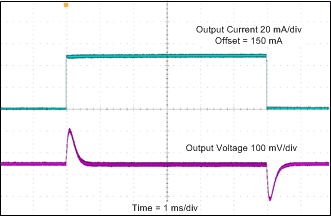
| VI = 3.3 V | VNEG = –10 V | |
| INEG = 150 mA to 200 mA | ||
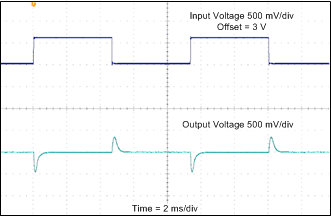
| VI = 3 V to 3.6 V | VNEG = –10 V | INEG = 100 mA |
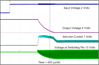
| VI = 3.3 V | VNEG = –10 V | INEG = 150 mA |
9.2.2 TPS65131-Q1 With VPOS = 5.5 V, VNEG = –5 V
9.2.2.1 Design Requirements
The design procedure for this setup is similar to the first example, see Detailed Design Procedure. Change the feedback dividers to set the output voltage, see Programming the Output Voltage. Further, choose the feed-forward capacitors according to Feedforward Capacitors. Table 5 shows the components being changed. See Figure 6.
Table 5. Design Parameters
| Design Parameter | Example Value | |||
|---|---|---|---|---|
| Input voltage range | 2.7 V to 5.5 V | |||
| Boost converter output voltage, VPOS | R1 = 390 kΩ R2 = 110 kΩ C9 = 18 pF |
5.5 V | ||
| Inverting converter output voltage, VNEG | R3 = 620 kΩ R4 = 150 kΩ C10 = 12 pF |
–5 V | ||
In this example, the converters are operated with power-save mode both enabled and disabled (see Power-Save Mode).
9.2.2.2 Application Curves
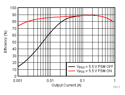
| VI = 3.3 V | VPOS = 5.5 V | Power-save mode on and off |
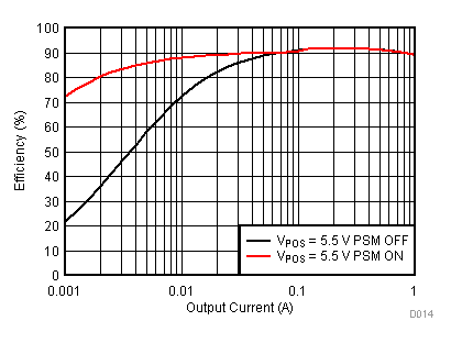
| VI = 5 V | VPOS = 5.5 V | Power-save mode on and off |
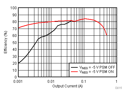
| VI = 3.3 V | VNEG = –5 V | Power-save mode on and off |
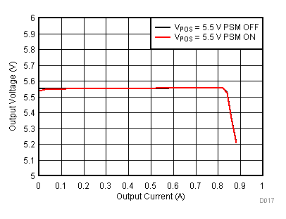
| VI = 3.3 V | VPOS = 5.5 V | Power-save mode on and off |
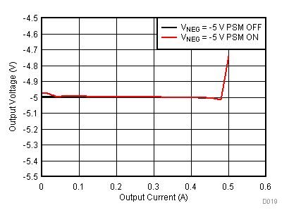
| VI = 3.3 V | VNEG = –5 V | Power-save mode on and off |
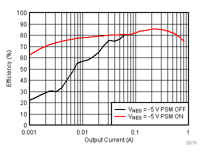
| VI = 5 V | VNEG = –5 V | Power-save mode on and off |
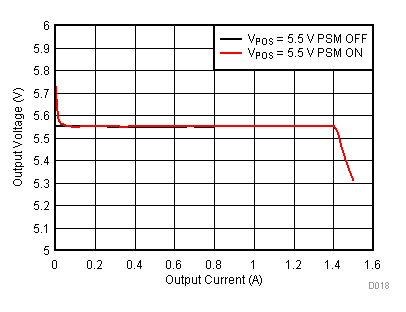
| VI = 5 V | VPOS = 5.5 V | Power-save mode on and off |
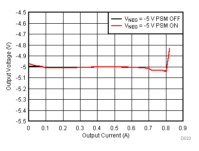
| VI = 3.3 V | VNEG = –5 V | Power-save mode on and off |
9.2.3 TPS65131-Q1 With VPOS = 15 V, VNEG = –15 V
9.2.3.1 Design Requirements
The design procedure for this setup is similar to the first example, see Detailed Design Procedure. Change the feedback dividers to set the output voltage, see Programming the Output Voltage. Further, choose the feedforward capacitors according to Feedforward Capacitors. Table 6 shows the components being changed. See Figure 6.
Table 6. Design Parameters
| Design Parameter | Example Value | |||
|---|---|---|---|---|
| Input voltage range | 2.7 V to 5.5 V | |||
| Boost converter output voltage, VPOS | R1 = 975 kΩ R2 = 85.8 kΩ C9 = 6.8 pF |
15 V | ||
| Inverting converter output voltage, VNEG | R3 = 1.3 MΩ R4 = 104.8 kΩ C10 = 5.6 pF |
–15 V | ||
In this example, the converters operate with power-save mode both enabled and disabled (see Power-Save Mode).
9.2.3.2 Application Curves
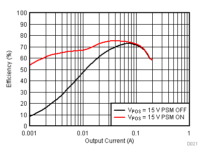
| VI = 3.3 V | VPOS = 15 V | Power-save mode on and off |
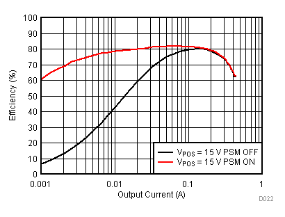
| VI = 5 V | VPOS = 15 V | Power-save mode on and off |
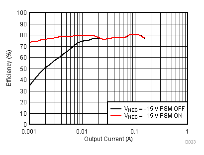
| VI = 3.3 V | VNEG = –15 V | Power-save mode on and off |
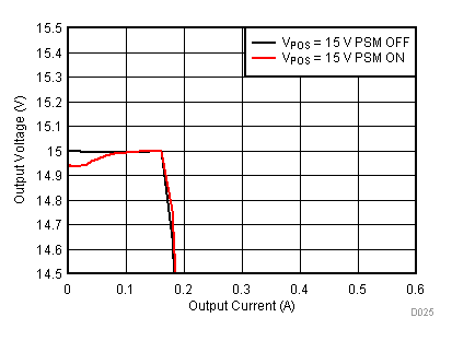
| VI = 3.3 V | VPOS = 15 V | Power-save mode on and off |
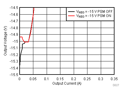
| VI = 3.3 V | VNEG = –15 V | Power-save mode on and off |
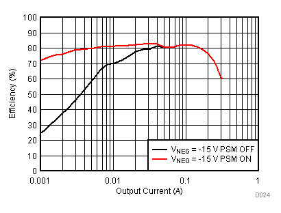
| VI = 5 V | VNEG = –15 V | Power-save mode on and off |
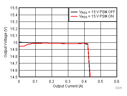
| VI = 5 V | VPOS = 15 V | Power-save mode on and off |
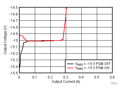
| VI = 5 V | VNEG = –15 V | Power-save mode on and off |
