JAJSK46A November 2020 – August 2021 TPS6521845
PRODUCTION DATA
- 1 特長
- 2 アプリケーション
- 3 概要
- 4 Revision History
- 5 Pin Configuration and Functions
- 6 Specifications
-
7 Detailed Description
- 7.1 Overview
- 7.2 Functional Block Diagram
- 7.3
Feature Description
- 7.3.1
Wake-Up and Power-Up and Power-Down Sequencing
- 7.3.1.1 Power-Up Sequencing
- 7.3.1.2 Power-Down Sequencing
- 7.3.1.3 Strobe 1 and Strobe 2
- 7.3.1.4 Supply Voltage Supervisor and Power-Good (PGOOD)
- 7.3.1.5 Backup Supply Power-Good (PGOOD_BU)
- 7.3.1.6 Internal LDO (INT_LDO)
- 7.3.1.7 Current Limited Load Switches
- 7.3.1.8 LDO1
- 7.3.1.9 Coin Cell Battery Voltage Acquisition
- 7.3.1.10 UVLO
- 7.3.1.11 Power-Fail Comparator
- 7.3.1.12 Battery-Backup Supply Power-Path
- 7.3.1.13 DCDC3 and DCDC4 Power-Up Default Selection
- 7.3.1.14 I/O Configuration
- 7.3.1.15 Push Button Input (PB)
- 7.3.1.16 AC_DET Input (AC_DET)
- 7.3.1.17 Interrupt Pin (INT)
- 7.3.1.18 I2C Bus Operation
- 7.3.1
Wake-Up and Power-Up and Power-Down Sequencing
- 7.4 Device Functional Modes
- 7.5 Register Maps
- 8 Application and Implementation
- 9 Power Supply Recommendations
- 10Layout
- 11Device and Documentation Support
- 12Mechanical, Packaging, and Orderable Information
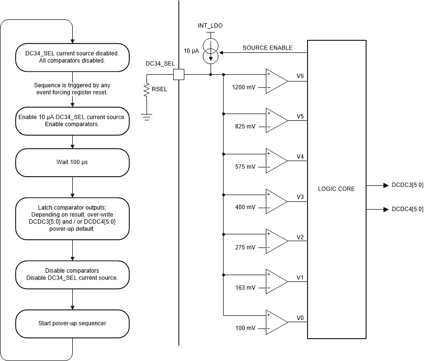
7.3.1.13 DCDC3 and DCDC4 Power-Up Default Selection
 Figure 7-22 Left:
Flow Chart for Selecting DCDC Power-Up Default Voltage Right: Comparator
Circuit
Figure 7-22 Left:
Flow Chart for Selecting DCDC Power-Up Default Voltage Right: Comparator
CircuitTable 7-1 Power-Up Default Values of
DCDC3 and DCDC4
| RSEL [KΩ] | POWER-UP DEFAULT | |||
|---|---|---|---|---|
| MIN | TYP | MAX | DCDC3[5:0] | DCDC4[5:0] |
| 0 | 0 | 7.7 | 0xCh (1.2 V) | 0x32h (3.3 V) |
| 11.3 | 12.1 | 13 | 0x12 (1.35 V) | 0x32h (3.3 V) |
| 18.1 | 20 | 22 | 0x18 (1.5 V) | 0x32h (3.3 V) |
| 30.9 | 31.6 | 32.3 | 0x1F (1.8 V) | 0x32h (3.3 V) |
| 44.8 | 45.3 | 46.4 | 0x3D (3.3 V) | 0x01 (1.2 V) |
| 64.2 | 64.9 | 0xCh (1.2 V)) | 0x07 (1.35 V) | |
| 92.9 | 95.3 | 96.9 | 0xCh (1.2 V) | 0x0D (1.5 V) |
| 135.3 | 150 | Tied to INT_LDO | 0xCh (1.2 V) | 0x14 (1.8 V) |