SLVSD66 September   2015 TPS65233-1

PRODUCTION DATA.  

  1. Features
  2. Applications
  3. Description
  4. Revision History
  5. Pin Configuration and Functions
  6. Specifications
    1. 6.1 Absolute Maximum Ratings
    2. 6.2 ESD Ratings
    3. 6.3 Recommended Operating Conditions
    4. 6.4 Thermal Information
    5. 6.5 Electrical Characteristics
    6. 6.6 I2C Interface Timing Requirements
    7. 6.7 Switching Characteristics
    8. 6.8 Typical Characteristics
  7. Detailed Description
    1. 7.1 Overview
    2. 7.2 Functional Block Diagram
    3. 7.3 Feature Description
      1. 7.3.1 Boost Converter
      2. 7.3.2 Linear Regulator and Current Limit
      3. 7.3.3 Charge Pump
      4. 7.3.4 Slew Rate Control
      5. 7.3.5 Short Circuit Protection, Hiccup, and Overtemperature Protection
    4. 7.4 Device Functional Modes
      1. 7.4.1 Tone Generation
      2. 7.4.2 Serial Interface
    5. 7.5 Programming
      1. 7.5.1 I2C Update Sequence
    6. 7.6 Register Map
      1. 7.6.1 Control Register 1 - Address: 0x00H
      2. 7.6.2 Control Register 2 - Address: 0x01H
      3. 7.6.3 Status Register 1 - Address: 0x02H
  8. Application and Implementation
    1. 8.1 Application Information
    2. 8.2 Typical Application
      1. 8.2.1 Detailed Design Procedure
        1. 8.2.1.1 Capacitor Selection
      2. 8.2.2 Application Curves
  9. Power Supply Recommendations
  10. 10Layout
    1. 10.1 Layout Guidelines
    2. 10.2 Layout Example
  11. 11Device and Documentation Support
    1. 11.1 Community Resources
    2. 11.2 Trademarks
    3. 11.3 Electrostatic Discharge Caution
    4. 11.4 Glossary
  12. 12Mechanical, Packaging, and Orderable Information

パッケージ・オプション

メカニカル・データ(パッケージ|ピン)
サーマルパッド・メカニカル・データ
発注情報

8 Application and Implementation

NOTE

Information in the following applications sections is not part of the TI component specification, and TI does not warrant its accuracy or completeness. TI’s customers are responsible for determining suitability of components for their purposes. Customers should validate and test their design implementation to confirm system functionality.

8.1 Application Information

TPS65233-1 is a monolithic voltage regulator, specifically to provide the 13-V/18-V power supply and the 22-kHz tone signaling to the LNB down-converter, with I2C interface. I2C GUI software is shared with TPS65233 which is available on ti.com.

8.2 Typical Application
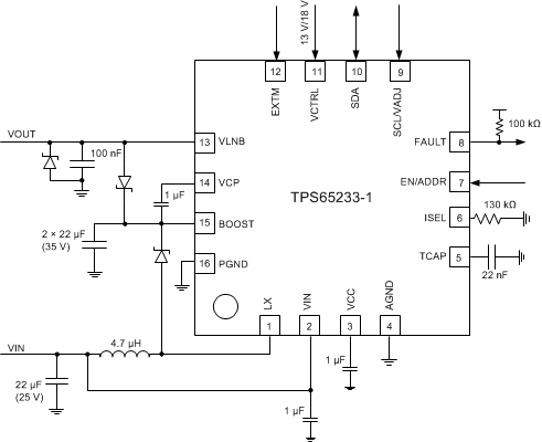
TPS65233-1 typ_app_LVSD66.gif Figure 15. Application Schematic

8.2.1 Detailed Design Procedure

8.2.1.1 Capacitor Selection

In TPS65233-1, a 1-MHz non-synchronous boost converter is integrated and the boost converter features the internal compensation network. 4.7 µH and 10 µH boost inductor are recommended. TPS65233-1 works fine with both ceramic capacitor and electrolytic capacitor. The ceramic capacitors rated at least X7R, 1206 size are preferred for the lower LNB output ripple. Table 8 shows the recommended ceramic capacitors list for both 4.7 µH and 10 µH boost inductors. Minimum output capacitor at the output of the boost converter is 2 × 10-µF/25-V ceramic capacitor when 4.7-µH inductor is selected.

Boost converter is stable with both ceramic capacitor and electrolytic capacitor. If lower cost is demanded, a 100-µF electrolytic and a 1-µF/35-V ceramic capacitor work well, this solution provides lower system cost.

Table 8. Boost Inductor and Capacitor Selections

BOOST INDUCTOR BOOST OUTPUT CAPACITOR (CERAMIC)
10 µH 2 × 22 µF, 25 V, 1206
2 × 10 µF, 35 V, 1206
1 × 22 µF, 35 V, 1206
2 × 22 µF, 35 V, 1206
4.7 µH 2 × 10 µF, 25 V, 1206
2 × 22 µF, 25 V, 1206
1 × 22 µF, 35 V, 1206
2 × 10 µF, 35 V, 1206
2 × 22 µF, 35 V, 1206

8.2.2 Application Curves
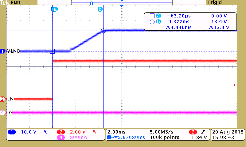
TPS65233-1 typ_curves_01_lvsd66.png
Figure 16. Soft Start, VLNB = 13.4 V, Delay from EN High to LNB Output High
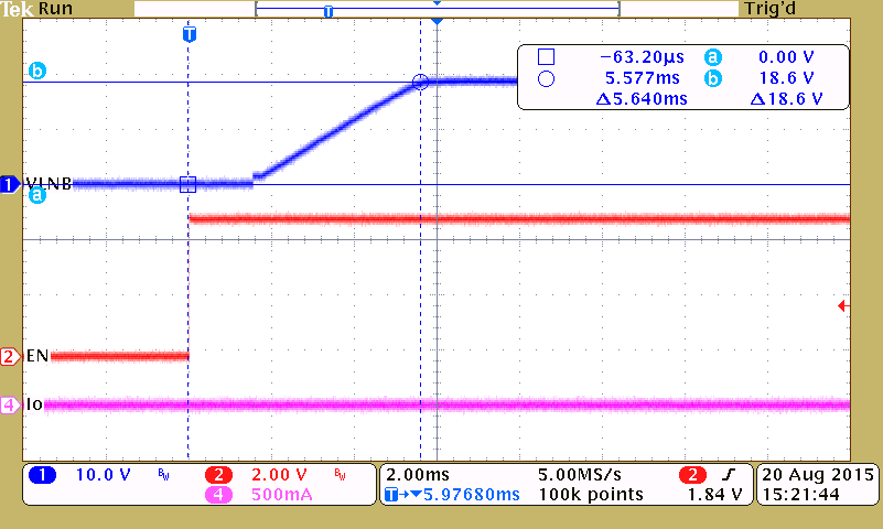
TPS65233-1 typ_curves_03_lvsd66.png
Figure 18. Soft Start, VLNB = 18.6 V, Delay from EN High to LNB Output High
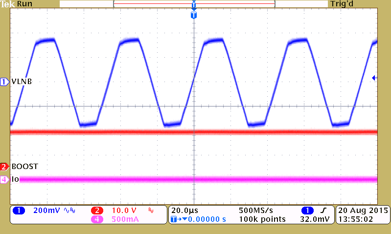
TPS65233-1 typ_curves_05_lvsd66.png
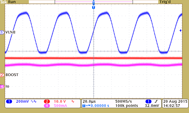
Figure 20. VLNB = 13.4 V, No Load, 22-kHz Tone
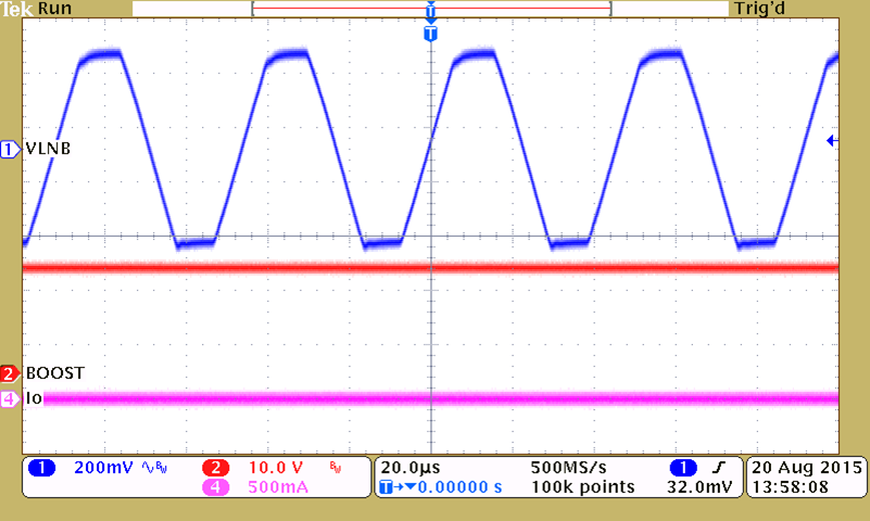
TPS65233-1 typ_curves_07_lvsd66.png
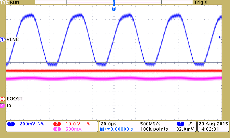
Figure 22. VLNB = 18.6 V, No Load, 22-kHz Tone
TPS65233-1 typ_curves_09_lvsd66.png
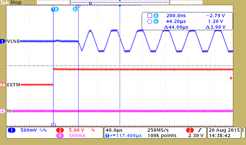
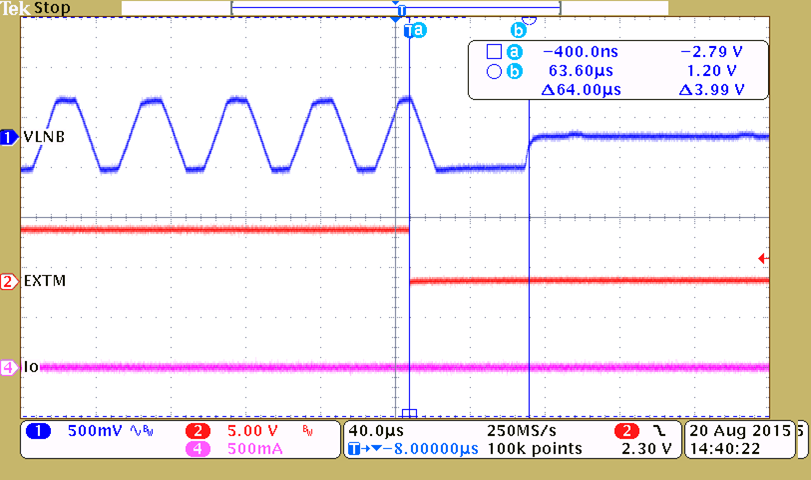
Figure 24. No Load, 22-kHz Tone Delay from EXTM Turns High to Output Tone, On
TPS65233-1 typ_curves_11_lvsd66.png
Figure 26. No Load, 22-kHz Tone Delay from EXTM Turns High to Output Tone, On
TPS65233-1 typ_curves_13_lvsd66.png
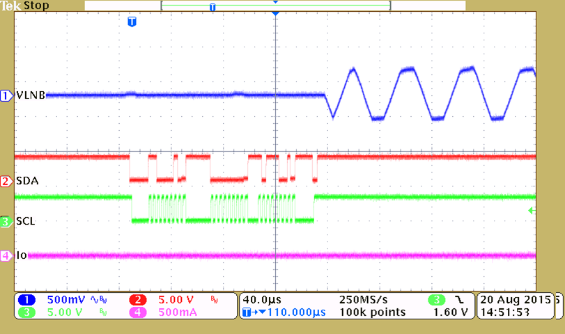
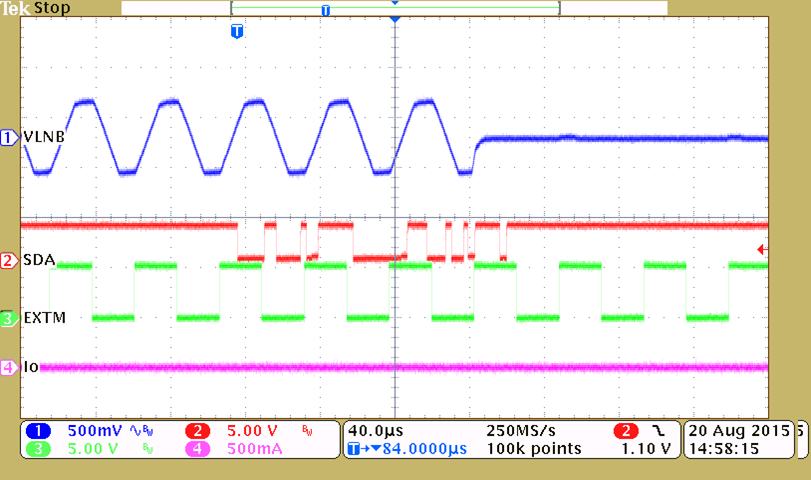
Figure 28. No Load, 22-kHz Tone Delay from I2C SDA to Output Tone, On
TPS65233-1 typ_curves_15_lvsd66.png
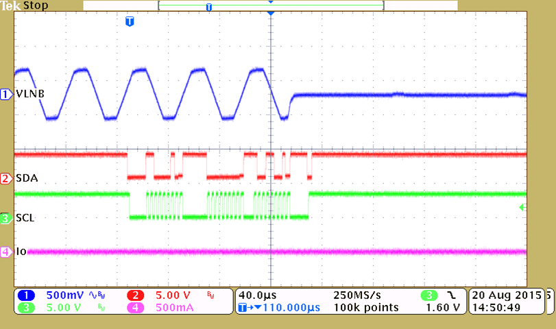
Figure 30. No Load, 22-kHz Tone Delay from I2C SDA to Output Tone, Off
TPS65233-1 typ_curves_02_lvsd66.png
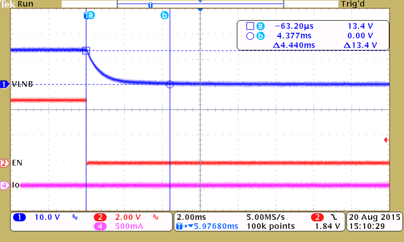
Figure 17. Power Off, VLNB = 13.4 V, Delay from EN Low to LNB Output Low
TPS65233-1 typ_curves_04_lvsd66.png
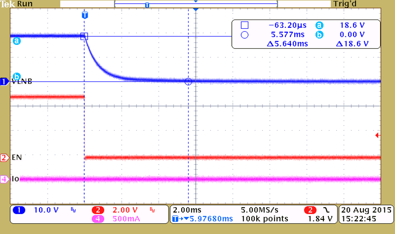
Figure 19. Power Off, VLNB = 18.6 V, Delay from EN Low to LNB Output Low
TPS65233-1 typ_curves_06_lvsd66.png
Figure 21. VLNB = 13.4 V, 950 mA, 22-kHz Tone
TPS65233-1 typ_curves_08_lvsd66.png
Figure 23. VLNB = 18.6 V, 950 mA, 22-kHz Tone
TPS65233-1 typ_curves_10_lvsd66.png
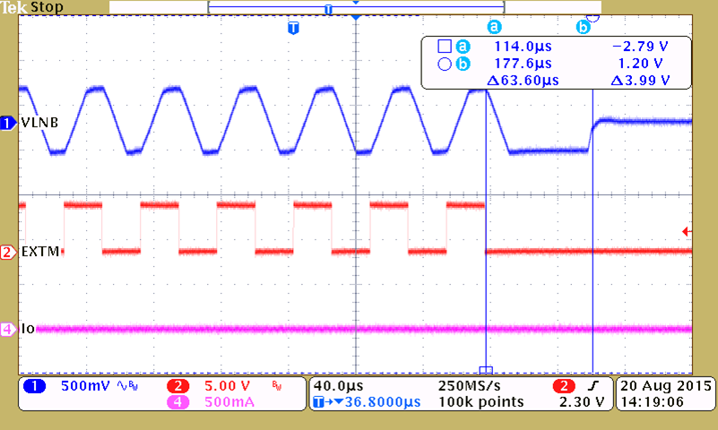
Figure 25. No Load, 22-kHz Tone Delay from EXTM Turns Low to Output Tone, Off
TPS65233-1 typ_curves_12_lvsd66.png
Figure 27. No Load, 22-kHz Tone Delay from EXTM Turns Low to Output Tone, Off
TPS65233-1 typ_curves_14_lvsd66.png
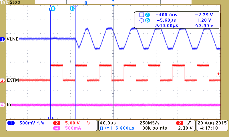
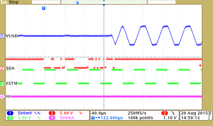
Figure 29. No Load, 22-kHz Tone Delay from I2C Gated, EXTM Provides 22 kHz to Output Tone, On
TPS65233-1 typ_curves_16_lvsd66.png
Figure 31. No Load, 22-kHz Tone Delay from I2C Gated, EXTM Provides 22 kHz to Output Tone, Off