SLVSCT9B November 2014 – January 2015 TPS65266
PRODUCTION DATA.
- 1 Features
- 2 Applications
- 3 Description
- 4 Revision History
- 5 Pin Configuration and Functions
- 6 Specifications
-
7 Detailed Description
- 7.1 Overview
- 7.2 Functional Block Diagram
- 7.3
Feature Description
- 7.3.1 Adjusting the Output Voltage
- 7.3.2 Enable and Adjusting UVLO
- 7.3.3 Soft-Start Time
- 7.3.4 Power-Up Sequencing
- 7.3.5 Boostrap Voltage and BST-LX UVLO
- 7.3.6 Out of Phase Operation
- 7.3.7 Output Overvoltage Protection (OVP)
- 7.3.8 Slope Compensation
- 7.3.9 Overcurrent Protection
- 7.3.10 Power Good
- 7.3.11 Adjustable Switching Frequency
- 7.3.12 Thermal Shutdown
- 7.4 Device Functional Modes
- 8 Application and Implementation
- 9 Power Supply Recommendations
- 10Layout
- 11Device and Documentation Support
- 12Mechanical, Packaging, and Orderable Information
パッケージ・オプション
メカニカル・データ(パッケージ|ピン)
- RHB|32
サーマルパッド・メカニカル・データ
- RHB|32
発注情報
6 Specifications
6.1 Absolute Maximum Ratings
over operating free-air temperature (unless otherwise noted) (1)| MIN | MAX | UNIT | ||
|---|---|---|---|---|
| Voltage at | VIN1, VIN2, VIN3, VINQ | –0.3 | 7 | V |
| LX1, LX2, LX3 (maximum withstand voltage transient <20 ns) | –1.0 | 7 | ||
| BST1, BST2, BST3 referenced to LX1, LX2, LX3 pins respectively | –0.3 | 7 | ||
| EN1, EN2, EN3, PGOOD | –0.3 | 7 | ||
| FB1, FB2, FB3, COMP1 , COMP2, COMP3, SS1, SS2, SS3, ROSC | –0.3 | 3.6 | ||
| AGND, PGND1, PGND2, PGND3 | –0.3 | 0.3 | ||
| TJ | Operating junction temperature | –40 | 150 | °C |
| Tstg | Storage temperature | –55 | 150 | °C |
(1) Stresses beyond those listed under Absolute Maximum Ratings may cause permanent damage to the device. These are stress ratings only, which do not imply functional operation of the device at these or any other conditions beyond those indicated under Recommended Operating Conditions. Exposure to absolute-maximum-rated conditions for extended periods may affect device reliability.
6.2 ESD Ratings
| VALUE | UNIT | |||
|---|---|---|---|---|
| V(ESD) | Electrostatic discharge | Human body model (HBM), per ANSI/ESDA/JEDEC JS-001, all pins(1) | ±2000 | V |
| Charged device model (CDM), per JEDEC specification JESD22-C101, all pins(2) | ±500 | |||
(1) JEDEC document JEP155 states that 500-V HBM allows safe manufacturing with a standard ESD control process.
(2) JEDEC document JEP157 states that 250-V CDM allows safe manufacturing with a standard ESD control process.
6.3 Recommended Operating Conditions
over operating free-air temperature range (unless otherwise noted)| MIN | MAX | UNIT | ||
|---|---|---|---|---|
| Voltage at | VIN1, VIN2, VIN3, VINQ | 2.7 | 6.5 | V |
| LX1, LX2, LX3 (maximum withstand voltage transient <20 ns) | –0.8 | 6.5 | ||
| BST1, BST2, BST3 referenced to LX1, LX2, LX3 pins respectively | –0.1 | 6.5 | ||
| EN1, EN2, EN3, PGOOD | –0.1 | 6.5 | ||
| FB1, FB2, FB3, COMP1 , COMP2, COMP3, SS1, SS2, SS3, ROSC | –0.1 | 3 | ||
| TJ | Operating junction temperature | –40 | 125 | °C |
6.4 Thermal Information
| THERMAL METRIC(1) | TPS65266 | UNIT | |
|---|---|---|---|
| RHB | |||
| 32 PINS | |||
| RθJA | Junction-to-ambient thermal resistance | 34.2 | °C/W |
| RθJC(top) | Junction-to-case (top) thermal resistance | 27.5 | |
| RθJB | Junction-to-board thermal resistance | 8.3 | |
| ψJT | Junction-to-top characterization parameter | 0.4 | |
| ψJB | Junction-to-board characterization parameter | 8.3 | |
| RθJC(bot) | Junction-to-case (bottom) thermal resistance | 2.8 | |
(1) For more information about traditional and new thermal metrics, see the IC Package Thermal Metrics application report, SPRA953.
6.5 Electrical Characteristics
TA = 25°C, VIN = 5 V, FSW = 1 MHz (unless otherwise noted)| PARAMETER | TEST CONDITIONS | MIN | TYP | MAX | UNIT | |
|---|---|---|---|---|---|---|
| INPUT SUPPLY VOLTAGE | ||||||
| VIN | Input voltage range | 2.7 | 6.5 | V | ||
| UVLO | VIN undervoltage lockout | VIN rising | 2.35 | 2.45 | 2.6 | V |
| VIN falling | 2.15 | 2.25 | 2.35 | V | ||
| Hysteresis | 200 | mV | ||||
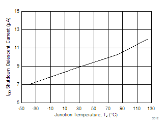
| IDDSDN | Shutdown supply current | EN1 = EN2 = EN3 = 0 V | 9 | µA | ||
| IDDQ_NSW | Input quiescent current without buck1/2/3 switching | EN1 = EN2 = EN3 = 5 V, FB1 = FB2 = FB3 = 0.8 V |
790 | µA | ||
| IDDQ_NSW1 | EN1 = 5 V, EN2 = EN3 = 0 V, FB1 = 0.8 V |
340 | µA | |||
| IDDQ_NSW2 | EN2 = 5 V, EN1 = EN3 = 0 V, FB2 = 0.8 V |
340 | µA | |||
| IDDQ_NSW3 | EN3 = 5 V, EN1 = EN2 = 0 V, FB3 = 0.8 V |
340 | µA | |||
| BUCK1, BUCK2, BUCK3 | ||||||
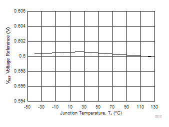
| VFB | Feedback voltage | VCOMP = 1.2 V | 0.594 | 0.6 | 0.606 | V |
| VENXH | EN1/2/3 high-level input voltage | 1.2 | 1.26 | V | ||
| VENXL | EN1/2/3 low-level input voltage | 1.1 | 1.15 | V | ||
| IENX1 | EN1/2/3 pullup current | ENx = 1 V | 1.8 | 2.1 | 2.4 | µA |
| IENX2 | EN1/2/3 pullup current | ENx = 1.3 V | 5.3 | µA | ||
| IENhys | Hysteresis current | 3.2 | µA | |||
| ISSX | Soft-start charging current | 4.5 | 5.5 | 6.5 | µA | |
| tON_MIN | Minimum on-time | 80 | 100 | ns | ||
| Gm_EA | Error amplifier transconductance | –2 µA < ICOMPX < 2 µA | 290 | µS | ||
| Gm_PS1/2/3 | COMP1/2/3 voltage to inductor current Gm(1) | ILX = 0.5 A | 10 | A/V | ||
| ILIMIT1 | Buck1 peak inductor current limit | 3.9 | 4.6 | 5.3 | A | |
| ILIMITSINK1 | Buck1 low-side sink current limit | 1.4 | ||||
| ILIMIT2/3 | Buck2/3 peak inductor current limit | 2.5 | 3.1 | 3.7 | A | |
| ILIMITSINK2/3 | Buck2/3 low-side sink current limit | 1.2 | A | |||
| Rdson_HS1 | Buck1 high-side switch resistance | VINQ = 5 V | 45 | mΩ | ||
| Rdson_LS1 | Buck1 low-side switch resistance | VINQ = 5 V | 50 | mΩ | ||
| Rdson_HS2 | Buck2 high-side switch resistance | VINQ = 5 V | 60 | mΩ | ||
| Rdson_LS2 | Buck2 low-side switch resistance | VINQ = 5 V | 60 | mΩ | ||
| Rdson_HS3 | Buck3 high-side switch resistance | VINQ = 5 V | 60 | mΩ | ||
| Rdson_LS3 | Buck3 low-side switch resistance | VINQ = 5 V | 60 | mΩ | ||
| HICCUP TIMING | ||||||
| tHiccup_wait | Overcurrent wait time(1) | 512 | cycles | |||
| tHiccup_re | Hiccup time before restart(1) | 16382 | cycles | |||
| POWER GOOD | ||||||
| Vth_PG | Feedback voltage threshold | FBx undervoltage falling | 92.5 | %VREF | ||
| FBx undervoltage rising | 95 | %VREF | ||||
| tDEGLITCH(PG)_F | PGOOD falling edge deglitch time | 128 | cycles | |||
| tRDEGLITCH(PG)_R | PGOOD rising edge deglitch time | 16350 | cycles | |||
| IPG | PGOOD pin leakage | 1 | µA | |||
| VLOW_PG | PGOOD pin low voltage | ISINK = 1 mA | 0.4 | V | ||
| OSCILLATOR | ||||||
| FSW | Switching frequency | ROSC = 51.1 kΩ | 920 | 1000 | 1080 | kHz |
| FSW_range | Switching frequency | 250 | 2400 | kHz | ||
| FSYNC | Clock sync frequency range | 250 | 2400 | kHz | ||
| tSYNC_w | Clock sync minimum pulse duration | 80 | ns | |||
| FSYNC_HI | Clock sync high threshold | 2 | V | |||
| VSYNC_LO | Clock sync low threshold | 0.4 | V | |||
| THERMAL PROTECTION | ||||||
| TTRIP_OTP(1) | Thermal protection trip point | Temperature rising | 160 | °C | ||
| THYST_OTP(1) | Hysteresis | 20 | °C | |||
(1) Lab validation result
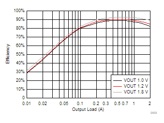
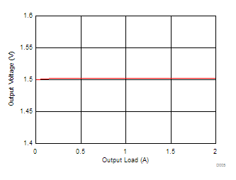
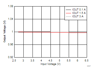
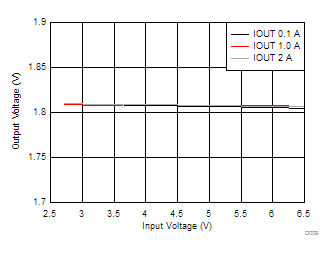
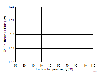
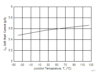
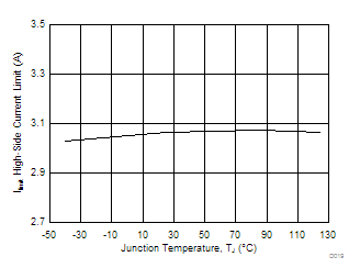
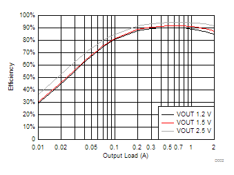
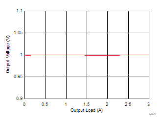
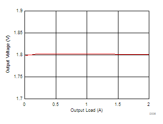
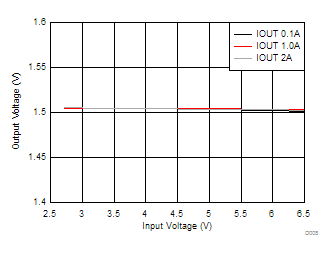
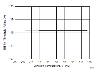
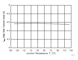
6.6 Typical Characteristics
TA = 25°C, VIN = 5 V, VOUT1 = 1.0 V, VOUT2 = 1.5 V, VOUT3 = 1.8 V FSW = 1 MHz (unless otherwise noted)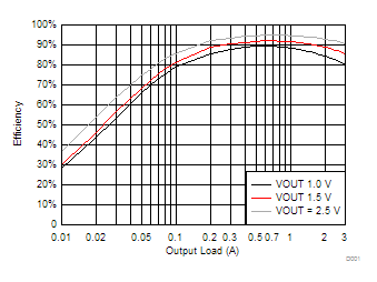
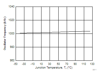
| ROSC = 51.1 kΩ | ||
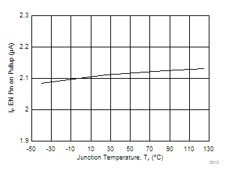
| VIN = 5 V | EN = 1 V | |
| VIN = 5 V | ||
| VIN = 5 V | ||
| VIN = 5 V | ||
| VIN = 5 V | ||
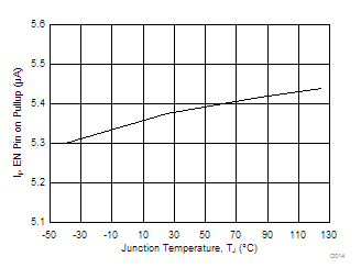
| VIN = 5 V | EN = 1.3 V | |
| VIN = 5 V | ||
| VIN = 5 V | ||

| VIN = 5 V | ||