SLVSBK1E September 2012 – May 2014 TPS65631
PRODUCTION DATA.
- 1 Features
- 2 Applications
- 3 Description
- 4 Simplified Schematic
- 5 Revision History
- 6 Pin Configuration and Functions
- 7 Specifications
-
8 Detailed Description
- 8.1 Overview
- 8.2 Functional Block Diagram
- 8.3 Feature Description
- 8.4 Device Functional Modes
- 9 Applications and Implementation
- 10Power Supply Recommendations
- 11Layout
- 12Device and Documentation Support
- 13Mechanical, Packaging, and Orderable Information
パッケージ・オプション
メカニカル・データ(パッケージ|ピン)
- DPD|12
サーマルパッド・メカニカル・データ
- DPD|12
発注情報
9 Applications and Implementation
9.1 Application Information
Figure 10 shows a typical application circuit suitable for supplying AMOLED displays in smartphone applications. The circuit is designed to operate from a single-cell Li-Ion battery and generates a positive output voltage VPOS of 4.6 V and a negative output voltage of –4 V. Both outputs are capable of supplying up to 300 mA of output current.
9.2 Typical Application
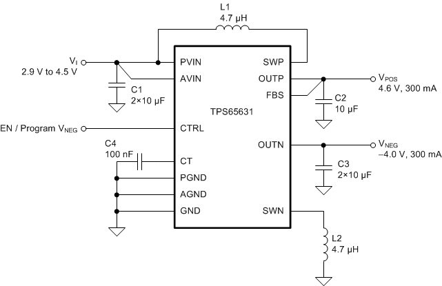 Figure 10. Typical Application Schematic
9.2.1 Design Requirements
For this design example, use the following input parameters.
Table 2. Design Parameters
| DESIGN PARAMETER | EXAMPLE |
|---|---|
| Input voltage range | 2.9 V to 4.5 V |
| Output voltage | VPOS = 4.6V, VNEG = –4 V |
| Switching frequency | 1.7 MHz |
9.2.2 Detailed Design Procedure
In order to maximize performance, the TPS65631 has been optimized for use with a relatively narrow range of component values, and customers are strongly recommended to use the application circuit shown in Figure 10 with the components listed in Table 3 and Table 4.
9.2.2.1 Inductor Selection
The boost converter and inverting buck-boost converter have been optimized for use with 4.7 µH inductors, and it is recommended that this value be used in all applications. Customers using other values of inductor are strongly recommended to characterize circuit performance on a case-by-case basis.
Table 3. Inductor Selection
| PARAMETER | VALUE | MANUFACTURER | PART NUMBER |
|---|---|---|---|
| L1, L2 | 4.7 µH | Coilmaster | MMPP252012-4R7N |
| Toko | 1239AS-H-4R7M | ||
| ABCO | LPP252012-4R7N | ||
| Coilcraft | XFL4020-4R7ML |
9.2.2.2 Capacitor Selection
The recommended capacitor values are shown in Table 4. Applications using less than the recommended capacitance (e.g. to save PCB area) may experience increased voltage ripple. In general, the lower the output power, the lower the necessary capacitance.
Table 4. Capacitor Selection
| PARAMETER | VALUE | MANUFACTURER | PART NUMBER |
|---|---|---|---|
| C1 | 2 × 10 µF | Murata | GRM21BR71A106KE51 |
| C2 | 10 µF | Murata | GRM21BR71A106KE51 |
| C3 | 2 × 10 µF | Murata | GRM21BR71A106KE51 |
| C4 | 100 nF | Murata | GRM21BR71E104KA01 |
9.2.3 Application Curves
The performance shown in the following graphs was obtained using the circuit shown in Figure 10 and the external components shown in Table 3 and Table 4. The output voltage settings for these measurements were VPOS = 4.6 V and VNEG = –4 V.
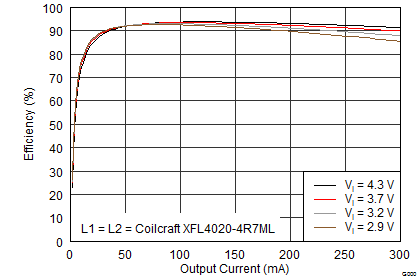
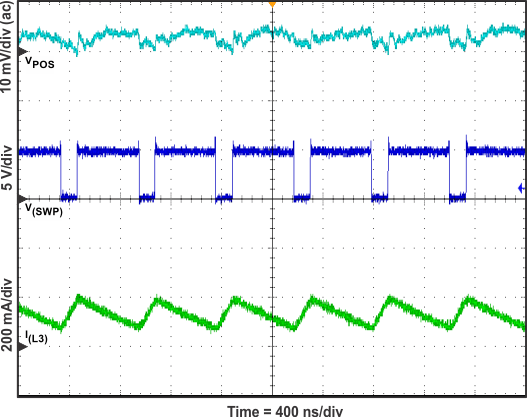 Figure 13. VPOS Switch Voltage, Inductor Current and Output Voltage Ripple (IO = 100 mA)
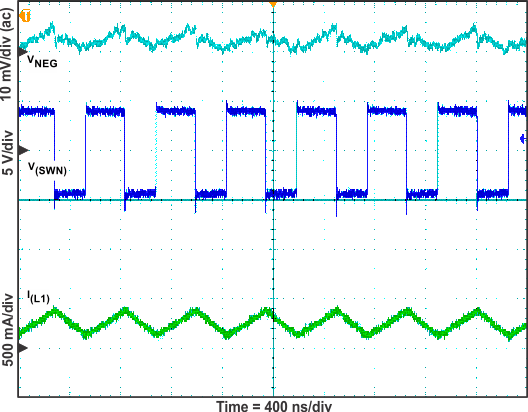 Figure 15. VNEG Switch Voltage, Inductor Current and Output Voltage Ripple (IO = 100 mA)
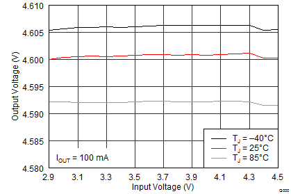
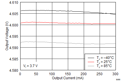
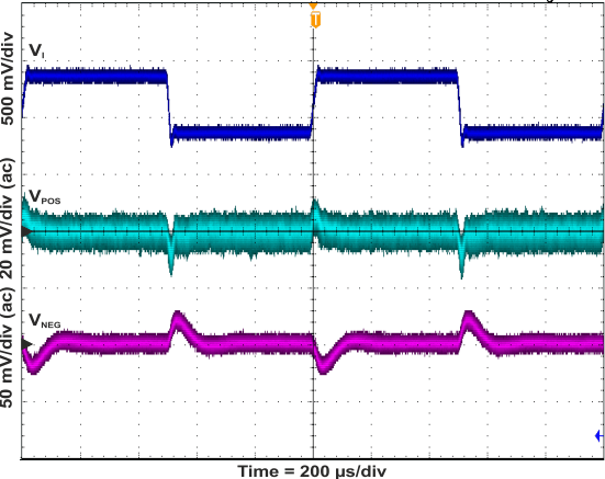 Figure 21. Line Transient Response
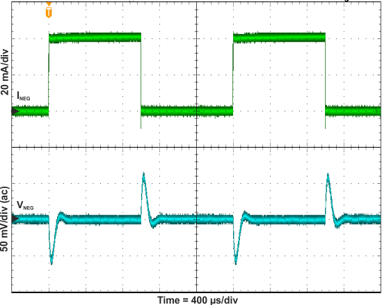 Figure 23. Inverting Buck-Boost Converter Load Transient Response
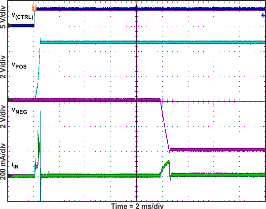 Figure 12. Start-Up Waveforms
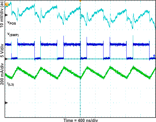 Figure 14. VPOS Switch Voltage, Inductor Current and Output Voltage Ripple (IO = 300 mA)
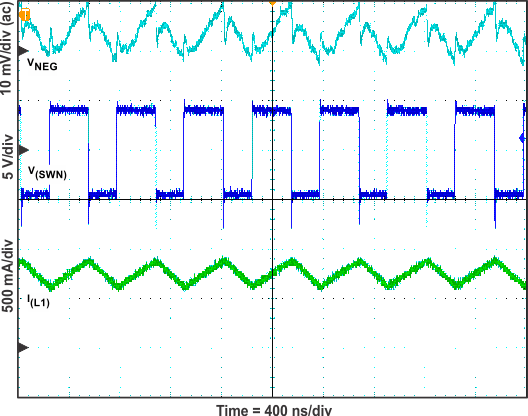 Figure 16. VNEG Switch Voltage, Inductor Current and Output Voltage Ripple (IO = 300 mA)
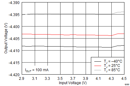
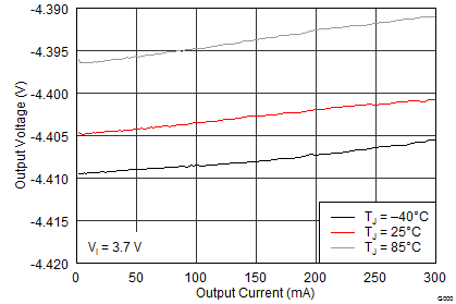
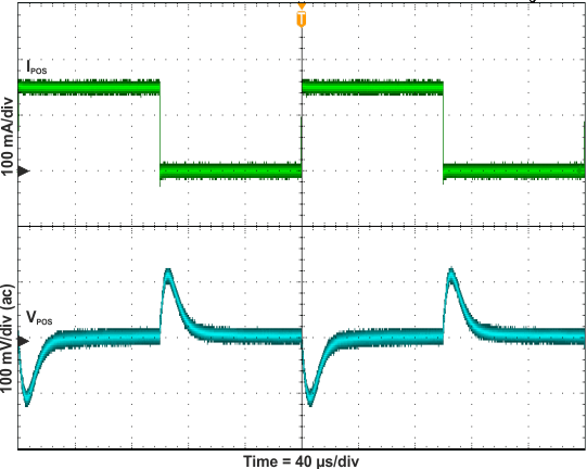 Figure 22. Boost Converter Load Transient Response