SLVSAE1B October 2010 – September 2015 TPS65708
PRODUCTION DATA.
- 1 Features
- 2 Applications
- 3 Description
- 4 Revision History
- 5 Pin Configuration and Functions
- 6 Specifications
- 7 Parameter Measurement Information
-
8 Detailed Description
- 8.1 Overview
- 8.2 Functional Block Diagram
- 8.3
Feature Description
- 8.3.1 DC-DC Converters
- 8.3.2 Power Save Mode
- 8.3.3 Dynamic Voltage Positioning
- 8.3.4 Soft Start
- 8.3.5 100% Duty Cycle Low Dropout Operation
- 8.3.6 180° Out-of-Phase Operation
- 8.3.7 Undervoltage Lockout and Enable for DCDC1, DCDC2, LDO1, and LDO2
- 8.3.8 Output Voltage Discharge
- 8.3.9 Power-Up Sequencing
- 8.3.10 Short-Circuit Protection
- 8.3.11 Thermal Shutdown
- 8.3.12 LDOs
- 8.3.13 LED Driver
- 8.4 Device Functional Modes
- 9 Application and Implementation
- 10Power Supply Recommendations
- 11Layout
- 12Device and Documentation Support
- 13Mechanical, Packaging, and Orderable Information
6 Specifications
6.1 Absolute Maximum Ratings
Over operating free-air temperature range (unless otherwise noted).(1)| MIN | MAX | UNIT | ||
|---|---|---|---|---|
| Voltage | All pins except A/PGND pins with respect to AGND | –0.3 | 7 | V |
| Pin VLDO1 and VLDO2 with respect to AGND | –0.3 | 3.6 | V | |
| Current | L1, L2, VLDO1, VLDO2, PGND | 700 | mA | |
| AGND, ISINK | 50 | mA | ||
| All other pins | 3 | mA | ||
| Operating free-air temperature, TA | –40 | 85 | °C | |
| Maximum junction temperature, TJ | 125 | °C | ||
| Storage temperature, Tstg | –65 | 150 | °C | |
(1) Stresses beyond those listed under Absolute Maximum Ratings may cause permanent damage to the device. These are stress ratings only and functional operation of the device at these or any other conditions beyond those indicated under Recommended Operating Conditions is not implied. Exposure to absolute-maximum-rated conditions for extended periods may affect device reliability.
6.2 ESD Ratings
| VALUE | UNIT | ||||
|---|---|---|---|---|---|
| V(ESD) | Electrostatic discharge | Human body model (HBM), per ANSI/ESDA/JEDEC JS-001(1) | ±2000 | V | |
| Charged device model (CDM), per JEDEC specification JESD22-C101(2) | ±500 | ||||
(1) JEDEC document JEP155 states that 500-V HBM allows safe manufacturing with a standard ESD control process.
(2) JEDEC document JEP157 states that 250-V CDM allows safe manufacturing with a standard ESD control process.
6.3 Recommended Operating Conditions
Over operating free-air temperature range (unless otherwise noted).| MIN | NOM | MAX | UNIT | ||
|---|---|---|---|---|---|
| VIN1/2 | Input voltage for step-down converter DCDC1and DCDC2 | 3.6 | 6 | V | |
| VOUTDCDC1/2 | Output voltage for DCDC1 and DCDC2 step-down converter | 0.8 | 3.3 | V | |
| IOUTDCDC1 | DC output current at L1 or L2 | 400 | mA | ||
| L | Inductor at L1 or L2(1) | 1 | 1.5 | 2.2 | µH |
| VINLDO1 | Input voltage for LDO1 | 1.7 | 6 | V | |
| VLDO | Output voltage for LDO1 and LDO2 | 0.8 | 3.3 | V | |
| VINLDO2 | Input voltage for LDO2 | 1.7 | 6 | V | |
| ILDO | Output current at LDO1 or LDO2 | 200 | mA | ||
| CINDCDC1/2 | Input capacitor at VIN1 and VIN2 | 4.7 | µF | ||
| COUTDCDC1/2 | Output capacitor at VOUT1, VOUT2 | 4.7 | 10 | 22 | µF |
| COUTLDO1/2 | Output capacitor at VLDO1, VLDO2 | 2.2 | µF | ||
| TA | Operating ambient temperature | –40 | 85 | °C | |
| TJ | Operating junction temperature | –40 | 125 | °C | |
(1) To support a typical inductor value of 1.5 µH, the minimum inductance can go as low as 1 µH. It is not recommended to use a 1-µH labeled inductor as the inductance will drop significantly below 1 µH in operation due to initial tolerances and saturation.
6.4 Thermal Information
| THERMAL METRIC(1) | TPS65708 | UNIT | |
|---|---|---|---|
| YZH (DSBGA) | |||
| 16 PINS | |||
| RθJA | Junction-to-ambient thermal resistance | 75 | °C/W |
| RθJC(top) | Junction-to-case (top) thermal resistance | 22 | °C/W |
| RθJB | Junction-to-board thermal resistance | 26 | °C/W |
| ψJT | Junction-to-top characterization parameter | 0.2 | °C/W |
| ψJB | Junction-to-board characterization parameter | 24 | °C/W |
| RθJC(bot) | Junction-to-case (bottom) thermal resistance | N/A | °C/W |
(1) For more information about traditional and new thermal metrics, see the Semiconductor and IC Package Thermal Metrics application report, SPRA953.
6.5 Electrical Characteristics
Unless otherwise noted: VIN1 = VIN2 = VCC = 5 V, L = 1.5 µH, COUTDCDCx = 10 µF, COUTLDOx = 2.2 µF, TA = –40°C to 85°C.| PARAMETER | TEST CONDITIONS | MIN | TYP | MAX | UNIT | |
|---|---|---|---|---|---|---|
| SUPPLY CURRENT | ||||||
| IQ | Operating quiescent current DCDCx and LDOx | DCDC1, DCDC2, LDO1 and LDO2 enabled, IOUT = 0 mA, MODE = 0; (PFM mode) ISINK in standby for PWM = 0 |
140 | 200 | μA | |
| DCDC1, DCDC2, LDO1 and LDO2 enabled, IOUT = 0 mA, MODE = 1 ; (PWM mode) ISINK in standby if PWM = 0; Not including inductor losses |
4 | mA | ||||
| DCDC1, DCDC2, LDO1 and LDO2 enabled, IOUT = 0 mA, MODE = 0; (PFM mode) ; ISINK in standby PWM = 0; During power-up sequencing |
170 | μA | ||||
| ISD | Shutdown Current | DCDCx, LDOx and ISINK disabled; VCC < 1.8 V |
6 | 15 | μA | |
| DIGITAL PINS ( MODE) | ||||||
| VIH | High-Level Input Voltage for MODE | 1.2 | VCC | V | ||
| VIL | Low-Level Input Voltage for MODE | 0 | 0.4 | V | ||
| Ilkg | Input Leakage Current | MODE tied to GND or VIN1 / VIN2 | 0.01 | 0.1 | μA | |
| UNDERVOLTAGE LOCKOUT (UVLO), SENSED AT PIN VCC | ||||||
| UVLO | Internal undervoltage lockout threshold | VCC, VIN1, VIN2 rising | 3.5 | 3.6 | 3.7 | V |
| Internal undervoltage lockout threshold hysteresis | VCC, VIN1, VIN2 falling | 130 | mV | |||
| STEP-DOWN CONVERTERS | ||||||
| VIN1 | Input voltage for DCDC1 | 3.5 | 6 | V | ||
| VIN2 | Input voltage for DCDC2 | 3.5 | 6 | V | ||
| POWER SWITCH | ||||||
| RDS(on) | High-side MOSFET ON-resistance | VIN1 / VIN2 = 3.6 V | 250 | 400 | mΩ | |
| Low-side MOSFET ON-resistance | VIN1 / VIN2 = 3.6 V | 150 | 300 | mΩ | ||
| ILIMF | Forward current limit | 3.6 V ≤ VIN1 / VIN2 ≤ 6 V | 650 | 820 | 1050 | mA |
| IO | DC output current | VIN1 / VIN2 > 3.5 V , L = 1.5 µH | 400 | mA | ||
| OSCILLATOR | ||||||
| fSW | Oscillator frequency | 2.03 | 2.25 | 2.48 | MHz | |
| OUTPUT | ||||||
| VOUT1 | DCDC1 default output voltage | VIN1 ≥ 3.6 V | 3.3 | V | ||
| VOUT2 | DCDC2 default output voltage | VIN2 ≥ 3.6 V | 1.8 | V | ||
| IFB | FB pin input current | DC-DC converter input voltage below undervoltage lockout threshold | 0.1 | µA | ||
| RFB | FB pin input resistance due to internal voltage divider | DC-DC converter input voltage above undervoltage lockout threshold; VOUT = 3.3 V | 990 | kΩ | ||
| RFB | FB pin input resistance due to internal voltage divider | DC-DC converter input voltage above undervoltage lockout threshold; VOUT = 1.8 V | 585 | kΩ | ||
| VOUT | DC output voltage accuracy(1) | VIN1 and VIN2 = 3.6 V to 6 V, +1% voltage positioning active; PFM operation, 0 mA < IOUT < IOUTmax |
1.25% | 3% | ||
| DC output voltage accuracy | VIN1 / VIN2 = 3.3V to 6V, PWM operation, 0 mA < IOUT < IOUTmax |
–1.5% | 1.5% | |||
| DC output voltage load regulation | PWM operation | 0.5 | %/A | |||
| tStart | Start-up time | Time from UVLO is exceeded (Vin > 3.6 V) to Start switching | 200 | µs | ||
| tRamp | VOUT ramp time | Time to ramp from 5% to 95% of VOUT | 250 | µs | ||
| RDIS | Internal discharge resistor at L1 and L2 | DCDCx disabled; 1 V < VIN1/2 < 3.6 V | 300 | 400 | 550 | Ω |
| THERMAL PROTECTION SEPARATELY FOR DCDC1, DCDC2 and LDO1 | ||||||
| TSD | Thermal shutdown | Increasing junction temperature | 150 | °C | ||
| Thermal shutdown hysteresis | Decreasing junction temperature | 30 | °C | |||
| VLDO1, VLDO2 LOW DROPOUT REGULATOR | ||||||
| VINLDO | Input voltage range for LDO1 and LDO2 | 1.7 | 6 | V | ||
| VLDO1 | LDO1 Default Output Voltage (1) | 2.8 | V | |||
| VLDO2 | LDO2 Default Output Voltage | 1.2 | V | |||
| IO | Output current for LDO1 and LDO2 | 200 | mA | |||
| ISC | LDO1 and LDO2 short circuit current limit | VLDOx = GND | 260 | 360 | 550 | mA |
| Dropout voltage at LDOx | IO = 200 mA; VINLDOx = 3.3 V | 200 | mV | |||
| Dropout voltage at LDOx | IO = 200 mA; VINLDOx = 1.8 V | 300 | mV | |||
| Output voltage accuracy for LDO1 and LDO2 | IO = 200 mA | –2% | 2% | |||
| Line regulation for LDO1 and LDO2 | VINLDO = VLDO + 0.5 V (min 1.7 V) to 6 V, IO = 50 mA |
–1% | 1% | |||
| Load regulation for LDO1 and LDO2 | IO = mA to 200 mA | –1.5% | 1% | |||
| PSRR | Power Supply Rejection Ratio | f = 10 kHz, COUT ≥ 2.2 μF VINLDOx = 5 V, VOUT = 2.8 V, IOUT = 100 mA | 50 | dB | ||
| Vn | Output noise voltage | VOUT = 2.8 V, BW = 10 Hz to 100 kHz | 160 | µV RMS | ||
| tRamp | VOUT ramp time | Internal soft start when LDO is enabled; Time to ramp from 5% to 95% of VOUT |
250 | µs | ||
| RDIS | Internal discharge resistor at VLDO1 and VLDO2 | VIN < UVLO | 200 | 400 | 550 | Ω |
| LED CURRENT SINK | ||||||
| ILED | Isink Current (LED current for 100% duty cycle) | Set internally by EEPROM to 7.5 mA; available current range from 7.5 mA to 30 mA; contact factory about default settings other than 7.5 mA | 7.5 | mA | ||
| Minimum voltage drop from ISINK to AGND needed for proper regulation | at 7.5 mA ≤ ISINK ≤ 20 mA | 0.4 | V | |||
| Minimum voltage drop from ISINK to AGND needed for proper regulation | at 20 mA < ISINK ≤ 30 mA | 0.55 | V | |||
| ISINK accuracy | ISINK ≥ 10 mA | –5% | 5% | |||
| ISINK accuracy | 7.5 mA ≤ ISINK < 10 mA | –10% | 10% | |||
| PWM duty cycle | 5% | 100% | ||||
| PWM frequency | 50 | kHz | ||||
| VIH | High-Level Input Voltage for PWM pin | ISINK is enabled | 1.2 | VCC | V | |
| VIL | Low-Level Input Voltage for PWM pin | ISINK is high resistive | 0 | 0.4 | V | |
| Ilkg | Input Leakage Current on PWM pin | 0.01 | 0.1 | μA | ||
| ISINK rise / fall time | V(ISINK) ≥ 0.4 V for 7.5 mA ≤ ISINK ≤ 20 mA; or V(ISINK) > 0.6 V for 20 mA < ISINK ≤ 30 mA |
500 | ns | |||
| ISINK rise / fall time | V(ISINK) ≤ 0.6 V; 20 mA < ISINK ≤ 30 mA | 700 | ns | |||
(1) VINLDO > 2.8 V
6.6 Typical Characteristics
Table 1. Table Of Graphs
| FIGURE | |||
|---|---|---|---|
| η | Efficiency DCDC (VO = 3.3 V) | vs Load current / PFM mode | Figure 1 |
| η | Efficiency DCDC (VO = 3.3 V) | vs Load current / PWM mode | Figure 2 |
| η | Efficiency DCDC (VO = 1.2 V) | vs Load current / PFM mode | Figure 3 |
| η | Efficiency DCDC (VO = 1.2 V) | vs Load current / PWM mode | Figure 4 |
| Line transient response DCDC (PWM) | Scope plot for a 3.6 V to 5 V to 3.6 V input voltage change | Figure 5 | |
| Line transient response DCDC (PFM) | Scope plot for a 3.6 V to 5 V to 3.6 V input voltage change | Figure 6 | |
| Line transient response LDO | Scope plot for a 3.6 V to 5 V to 3.6 V input voltage change | Figure 7 | |
| Load transient response DCDC (PFM) | Scope plot for a 10% to 90% load step (40 mA to 360 mA) | Figure 8 | |
| Load transient response DCDC (PWM) | Scope plot for a 10% to 90% load step (40 mA to 360 mA) | Figure 9 | |
| Load transient response LDO | Scope plot for a 10% to 90% load step (20 mA to 180 mA) | Figure 10 | |
| Startup timing DCDC1, DCDC2, LDO1 and LDO2 | Scope plot of startup; R1 = supply voltage is applied | Figure 14 | |
| LDO POWER SUPPLY REJECTION RATIO (PSRR) | Scope plot | Figure 11 | |
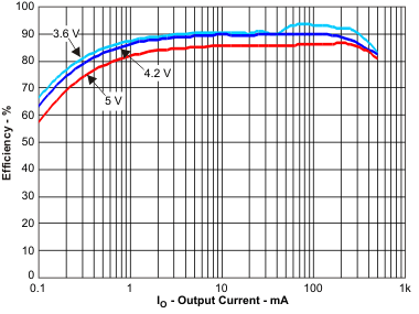 Figure 1. Efficiency DCDC (VO = 3.3 V) vs Load Current / PFM Mode; for VIN = 3.6 V to 5 V
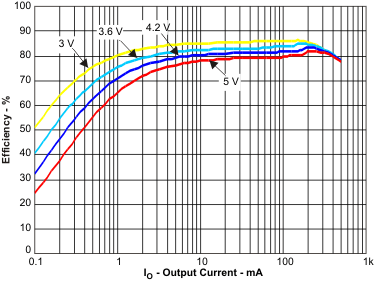 Figure 3. Efficiency DCDC (VO = 1.2 V) vs Load Current / PFM Mode; for VIN = 3 V to 5 V
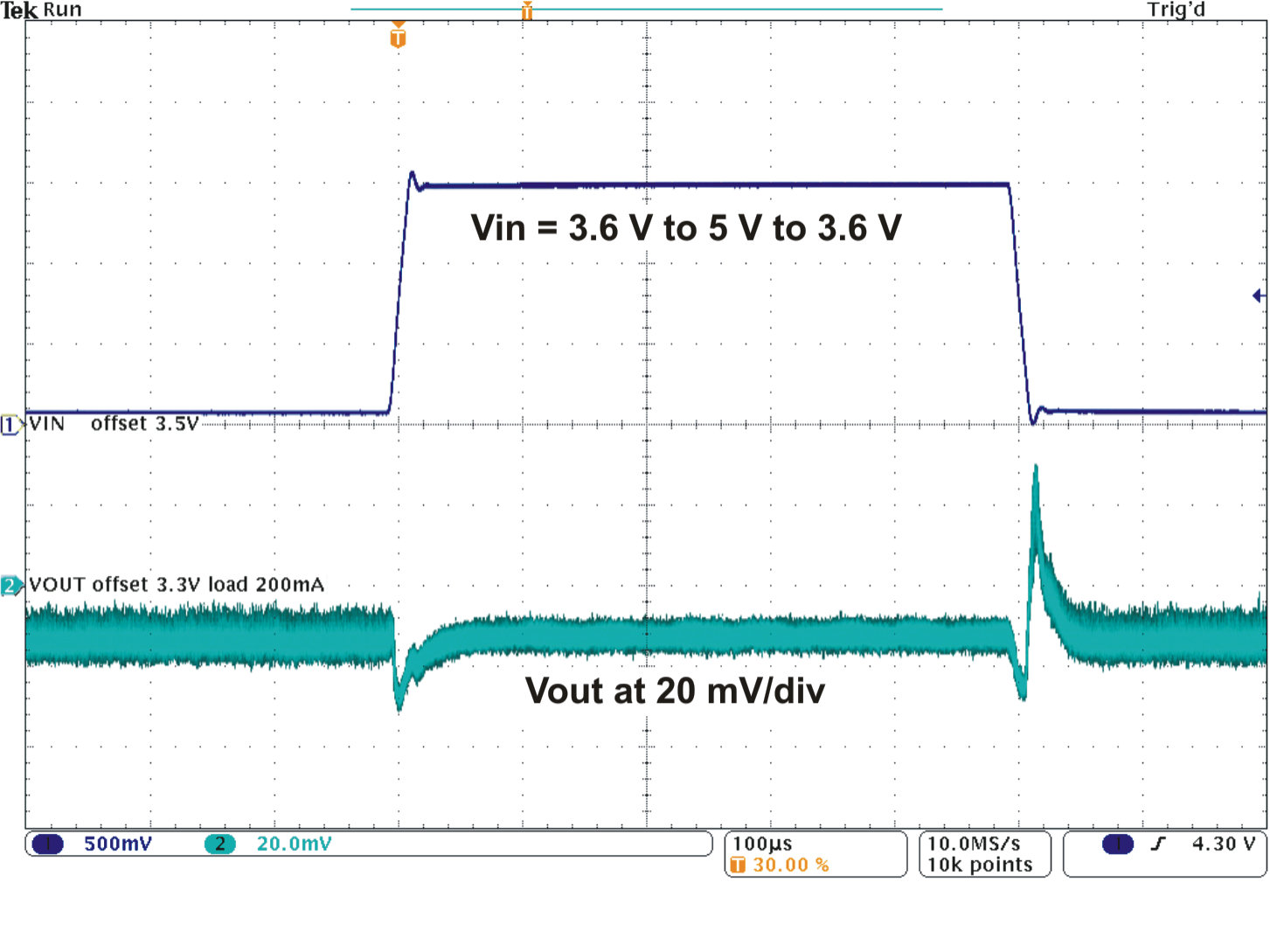 Figure 5. Line Transient Response DCDC (PWM)
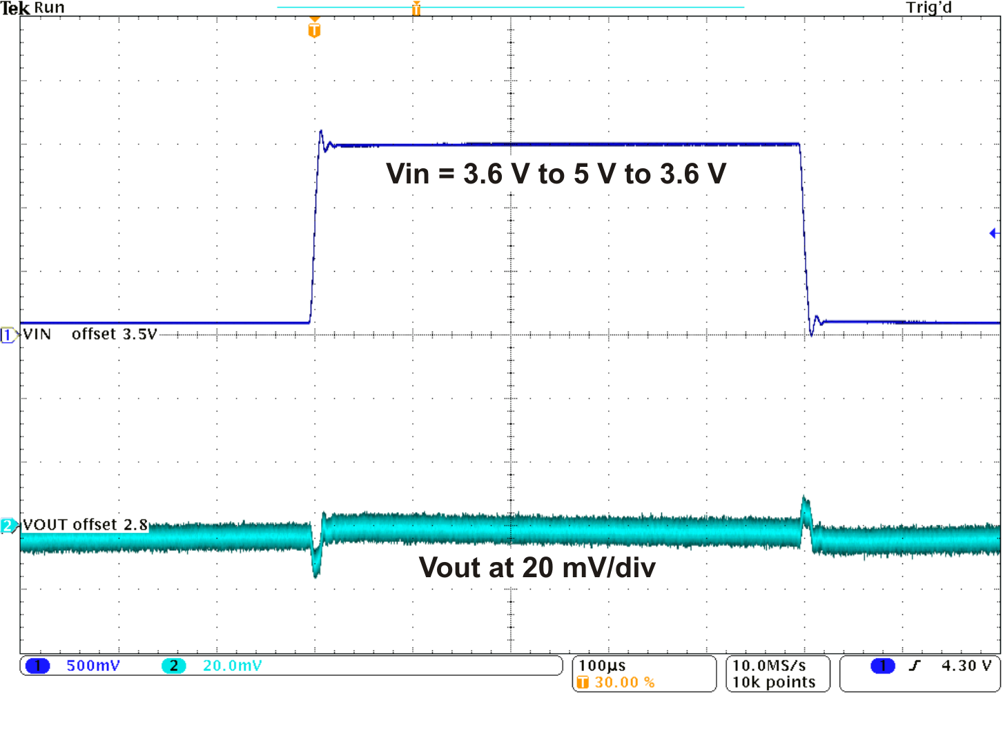 Figure 7. Line Transient Response LDO
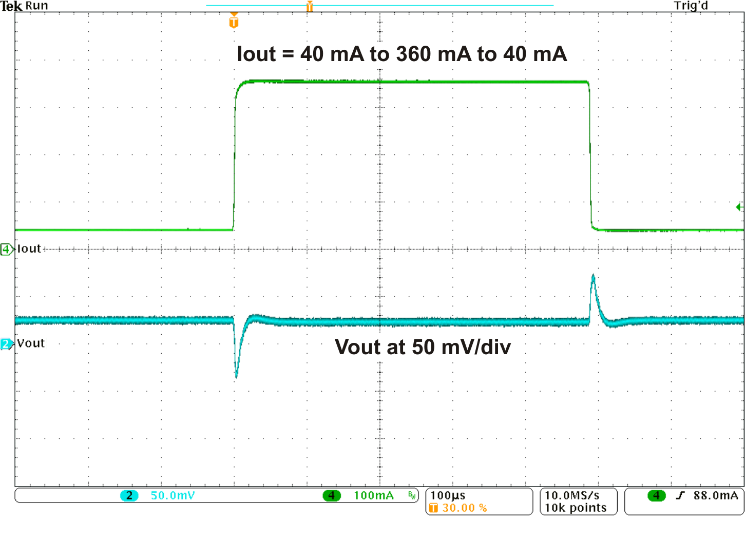 Figure 9. Load Transient Response DCDC (PWM)
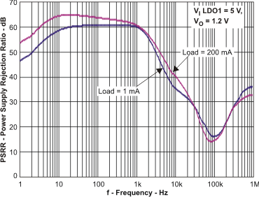
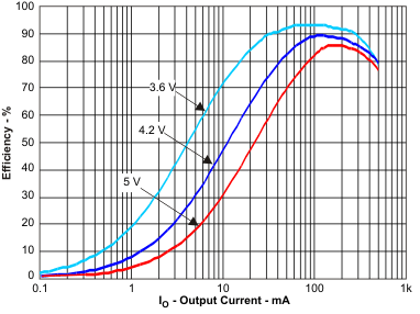 Figure 2. Efficiency DCDC (VO = 3.3 V) vs Load Current / PWM Mode; for VIN = 3.6 V to 5 V
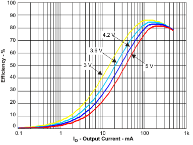 Figure 4. Efficiency DCDC (VO = 1.2 V) vs Load Current / PWM Mode; for VIN = 3 V to 5 V
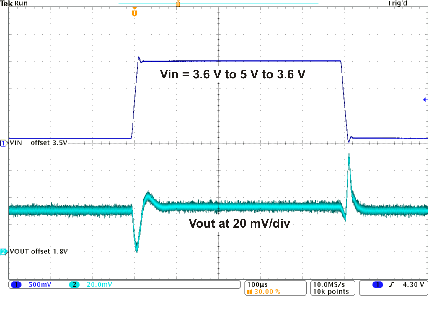 Figure 6. Line Transient Response DCDC (PFM)
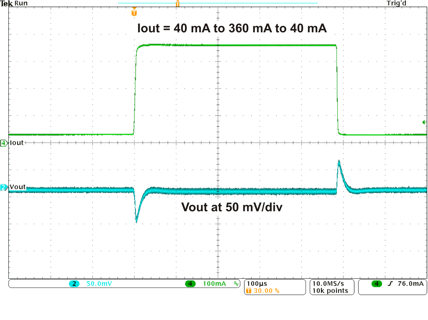 Figure 8. Load Transient Response DCDC (PFM)
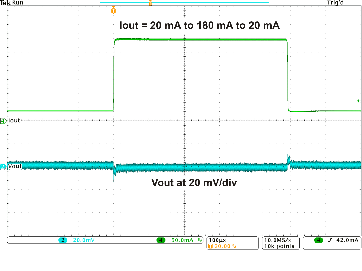 Figure 10. Load Transient Response LDO