SLVSCW2A September   2015  – February 2016 TPS657095

PRODUCTION DATA.  

  1. Features
  2. Applications
  3. Description
  4. Revision History
  5. Pin Configuration and Functions
  6. Specifications
    1. 6.1 Absolute Maximum Ratings
    2. 6.2 ESD Ratings
    3. 6.3 Recommended Operating Conditions
    4. 6.4 Thermal Information
    5. 6.5 Electrical Characteristics
    6. 6.6 Timing Requirements
    7. 6.7 Typical Characteristics
  7. Detailed Description
    1. 7.1 Overview
    2. 7.2 Functional Block Diagram
    3. 7.3 Feature Description
      1. 7.3.1  State Diagram
      2. 7.3.2  Power-up Timing
      3. 7.3.3  GPO
      4. 7.3.4  GPIO
      5. 7.3.5  LED_EN
      6. 7.3.6  PWM Dimming
      7. 7.3.7  Crystal Oscillator and CLKOUT
      8. 7.3.8  LDOs
      9. 7.3.9  Undervoltage Lockout
      10. 7.3.10 Power Up/Power Down Default States
      11. 7.3.11 Output Voltage Discharge for LDO1 and LDO2
      12. 7.3.12 Power-Good Status Bits for LDO1 and LDO2
      13. 7.3.13 Short-Circuit Protection
      14. 7.3.14 Thermal Shutdown
      15. 7.3.15 LED Driver
      16. 7.3.16 4kByte OTP Memory
        1. 7.3.16.1 Programming the 4KByte OTP Memory
    4. 7.4 Device Functional Modes
      1. 7.4.1 Shutdown Mode
      2. 7.4.2 Operational Mode
    5. 7.5 Programming
      1. 7.5.1 Serial Interface
    6. 7.6 Register Map
      1. 7.6.1  DEV_AND_REV_ID Register Address: 00h
      2. 7.6.2  OTP_REV Register Address: 01h
      3. 7.6.3  GPIO_CTRL Register Address: 02h
      4. 7.6.4  PWM_OSC_CNTRL Register Address: 03h
      5. 7.6.5  ISINK_CURRENT Register Address: 04h
      6. 7.6.6  LDO_CTRL Register Address: 05h
      7. 7.6.7  LDO1_VCTRL Register Address: 06h
      8. 7.6.8  LDO2_VCTRL Register Address: 07h
      9. 7.6.9  PWM_DUTY_THR_L Register Address: 08h
      10. 7.6.10 PWM_DUTY_THR_H Register Address: 09h
      11. 7.6.11 RESERVED Register Address: 0Ah
      12. 7.6.12 PWM_DUTY_L Register Address: 0Bh
      13. 7.6.13 PWM_DUTY_H Register Address: 0Ch
      14. 7.6.14 RESERVED Register Address: 0Dh
      15. 7.6.15 SPARE Register Address: 0Eh
      16. 7.6.16 4K_OTP_PASSWORD Register Address: 0Fh
  8. Application and Implementation
    1. 8.1 Application Information
    2. 8.2 Typical Application
      1. 8.2.1 Design Requirements
      2. 8.2.2 Detailed Design Procedure
        1. 8.2.2.1 Output Capacitor Selection
        2. 8.2.2.2 Input Capacitor Selection
      3. 8.2.3 Application Curves
  9. Power Supply Recommendations
  10. 10Layout
    1. 10.1 Layout Guidelines
    2. 10.2 Layout Example
  11. 11Device and Documentation Support
    1. 11.1 Device Support
      1. 11.1.1 Third-Party Products Disclaimer
    2. 11.2 Community Resources
    3. 11.3 Trademarks
    4. 11.4 Electrostatic Discharge Caution
    5. 11.5 Glossary
  12. 12Mechanical, Packaging, and Orderable Information
    1. 12.1 Package Summary
    2. 12.2 Chip Scale Package Dimensions

パッケージ・オプション

メカニカル・データ(パッケージ|ピン)
サーマルパッド・メカニカル・データ
発注情報

6 Specifications

6.1 Absolute Maximum Ratings

over operating free-air temperature range (unless otherwise noted)(1)
MIN MAX UNIT
Voltage All pins except GND pin with respect to AGND –0.3 7 V
GPIO and GPO pull-up voltage if configured as open drain output -0.3 VCC + 0.3 V
Pin VLDO1 and VLDO2 with respect to AGND –0.3 3.6 V
Current VLDO1, VLDO2, VCC 200 mA
GND, ISINK, GPIO, GPO 50 mA
All other pins 3 mA
Operating free-air temperature, TA –40 85 °C
Maximum junction temperature, TJ 125 °C
Storage temperature range, Tstg –65 150 °C
(1) Stresses beyond those listed under absolute maximum ratings may cause permanent damage to the device. These are stress ratings only and functional operation of the device at these or any other conditions beyond those indicated under recommended operating conditions is not implied. Exposure to absolute-maximum-rated conditions for extended periods may affect device reliability.

6.2 ESD Ratings

VALUE UNIT
V(ESD) Electrostatic discharge Human body model (HBM), per ANSI/ESDA/JEDEC JS-001(1) 2000 V
Charged device model (CDM), per JEDEC specification JESD22-C101(2) 500 V
(1) JEDEC document JEP155 states that 500-V HBM allows safe manufacturing with a standard ESD control process.
(2) JEDEC document JEP157 states that 250-V CDM allows safe manufacturing with a standard ESD control process.

6.3 Recommended Operating Conditions

over operating free-air temperature range (unless otherwise noted)
MIN NOM MAX UNIT
VCC /AVCC Input voltage range 3.7 6 V
CVCC Input capacitor at VCC 1 µF
CAVCC Input capacitor at AVCC 1 µF
VLDOx Output voltage range for LDO1 and LDO2 0.8 3.3 V
ILDO Output current at LDO1 or LDO2 75 mA
COUTLDO1/2 Output capacitance at VLDO1, VLDO2 2.2 6.8 µF
LED_EN Voltage range 1.3 6 V
GPIO Voltage range (configured as an input) 1.3 3.3 V
TA Operating ambient temperature –40 85 °C
TJ Operating junction temperature –40 125 °C

6.4 Thermal Information

THERMAL METRIC(1) TPS657095 UNIT
YFF (DSBGA)
16 PINS
RθJA Junction-to-ambient thermal resistance 78.2 °C/W
RθJC(top) Junction-to-case (top) thermal resistance 0.6
RθJB Junction-to-board thermal resistance 13.2
ψJT Junction-to-top characterization parameter 2.5
ψJB Junction-to-board characterization parameter 13
RθJC(bot) Junction-to-case (bottom) thermal resistance n/a
(1) For more information about traditional and new thermal metrics, see the IC Package Thermal Metrics application report, SPRA953.

6.5 Electrical Characteristics

Unless otherwise noted: VCC = AVCC = 5V, CVCC = 1µF; COUTLDOx= 2.2µF, TA = –40°C to 85°C
PARAMETER TEST CONDITIONS MIN TYP MAX UNIT
SUPPLY CURRENT
VCC, AVCC Supply voltage During normal operation 3.7 6 V
During programming (writing) of OTP memory -5% 5 +5% V
IQ Operating quiescent current LDO1 disabled
LDO2 disabled
No I2C communications
LED_EN = 0
CLKout_EN = 0
24MHz crystal disabled
25 30 μA
LDO1 disabled
LDO2 enabled, IOUT(LDO2) = 0 mA
No I2C communications
LED_EN = 0
CLKout_EN = 0
24MHz crystal disabled
40 55 uA
LDO1 enabled, IOUT(LDO1) = 0 mA
LDO2 disabled
No I2C communications
LED_EN = 0
CLKout_EN = 0
24MHz crystal disabled
40 55 μA
LDO1 enabled, IOUT(LDO1) = 0 mA
LDO2 enabled, IOUT(LDO2) = 0 mA
No I2C communications
LED_EN = 0
CLKout_EN = 0
24MHz crystal disabled
60 80 μA
LDO1 enabled, IOUT(LDO1) = 0 mA
LDO2 enabled, IOUT(LDO2) = 0 mA
No I2C communications
LED_EN = 0
CLKout_EN = 1
24MHz crystal enabled
2900 3550 μA
LDO1 enabled, IOUT(LDO1) = 0 mA
LDO2 enabled, IOUT(LDO2) = 0 mA
No I2C communications
LED_EN = 1, PWM Duty Cycle set to 99.9%, ISINK = 2mA
CLKout_EN = 1
24MHz crystal enabled
3000 3600 μA
ISD Shutdown current Device disabled;
VCC and AVCC < 1.8V
45 85 μA
LED_ENABLE
VIH High level input voltage 1.1 VCC V
VIL Low level input voltage 0.4 V
I(in)lkg Input Leakage Current 0.1 μA
Input Deglitch With a minimum pulse period of 500ns before another glitch is received 100 ns
GENERAL PURPOSE INPUT/OUTPUT (GPIO)
VIH High level input voltage For VLDO1 = 1.8V 1.1 VLDO1 V
VIH High level input voltage For VLDO1 = 3.3V 1.37 VLDO1 V
VIL Low level input voltage For VLDO1 = 1.8V 0 0.4 V
VIL Low level input voltage For VLDO1 = 3.3V 0 0.6 V
I(in)lkg Input leakage current GPIO programmed as input and tied to GND or VCC 0.01 0.1 μA
VOH High level output voltage Configured as a push-pull output, IOH = 1mA, VLDO1 ≥ 1.8V 1.2 VLDO1-0.2V VLDO1 V
VOH High level output voltage Configured as a push-pull output, IOH = 1mA, 1.3V ≤ VLDO1 ≤1.8V 1.0 VLDO1 V
VOL Low level output voltage Configured as a push-pull output, IOL= 2mA, VLDO1 ≥ 1.8V 0.25 V
VOL Low level output voltage Configured as a push-pull output, IOL= 2mA, 1.3V ≤ VLDO1 ≤1.8V 0.3 V
VOL Low level output voltage Configured as an open-drain output, IOL= 4mA, VLDO1 ≥ 1.8V 0.6 V
VOL Low level output voltage Configured as an open-drain output, IOL= 2mA, 1.3V ≤ VLDO1 ≤1.8V 0.6 V
I(out)lkg Output leakage current Configured as an open-drain output, GPIO connected to VLDO1 0.01 0.1 μA
GENERAL PURPOSE OUTPUT (GPO)
VOH High level output voltage Configured as a push-pull output, IOH = 1mA, VLDO1 ≥ 1.8V 1.2 VLDO1-0.2V VLDO1 V
VOH High level output voltage Configured as a push-pull output, IOH = 1mA, 1.3V ≤ VLDO1 ≤ 1.8V 1.0 VLDO1 V
VOL Low level output voltage Configured as a push-pull output, IOL= 2mA, VLDO1 ≥ 1.8V 0.25 V
VOL Low level output voltage Configured as a push-pull output, IOL= 2mA, 1.3V ≤ VLDO1 ≤ 1.8V 0.3 V
VOL Low level output voltage Configured as an open-drain output, IOL= 4mA, VLDO1 ≥ 1.8V 0.6 V
VOL Low level output voltage Configured as an open-drain output, IOL= 2mA, 1.3V ≤ VLDO1 ≤1.8V 0.6 V
I(out)lkg Output leakage current Configured as an open-drain output, GPO connected to VLDO1 0.01 0.1 μA
SCL, SDA
VIH High level input voltage on SCL, SDA 1.2 Vcc V
VIL Low level input voltage on SCL, SDA 0 0.4 V
Ilkg Pin leakage current on SCL, SDA (includes leakage current for the open-drain output) Input at VIL or VIH 100 nA
VOL Low level output voltage on SDA For IOL= 1mA 0.25 V
UNDERVOLTAGE LOCKOUT (UVLO), SENSED AT PIN AVCC
UVLO Internal undervoltage lockout threshold AVCC rising 3.4 3.6 3.7 V
Internal undervoltage lockout threshold hysteresis AVCC falling 130 mV
CLOCK GENERATOR
fosc Frequency of external crystal 24 MHz
fCLKOUT Frequency on pin CLKOUT For OSC_FREQ[1,0] = 00 24 MHz
For OSC_FREQ[1,0] = 01 12
For OSC_FREQ[1,0] = 10 6
For OSC_FREQ[1,0] = 11 3
Period jitter; rms Measured period compared to the Average Period of 10,000 randomly selected cylces 600 ps
Peak period to period jitter Measured period compared to the Average Period of 10,000 randomly selected cylces 600 ps
Duty cycle of CLKout 40% 50% 60%
Rise time / fall time for clock output 10% to 90% of output voltage, 1.3V ≤ VLDO1 ≤ 3.3V 10 ns
Load capacitance Defines the maximum capacitance that can be driven by the CLKOUT buffer and still meet the specified rise/fall times 15 pF
Output impedance 50 Ω
VOH High level output voltage Internally connected to VLDO1≥ 1.8V: for COUT = 15pF, IOH = 1mA 1.6 VLDO1
- 0.2V
VLDO1 V
VOL Low level output voltage For COUT = 15pF, IOL = 1mA 0.2 0.3 V
tstart Oscillator start-up time Time from CLKout_EN=1 to CLKout active for the NXTBD-24.000M crystal, not tested in production but based on simulations 10 ms
THERMAL PROTECTION
TSD Thermal shutdown Increasing junction temperature 150 °C
Thermal shutdown hysteresis Decreasing junction temperature 30 °C
VLDO1, VLDO2 LOW DROPOUT REGULATORS
VCC Input voltage range for LDO1 and LDO2 3.7 6 V
VLDO1 LDO1 output voltage See LDO1_CTRL Register definition for all available voltage settings. 0.8 1.8 3.3 V
VLDO2 LDO2 output voltage See LDO2_CTRL Register definition for all available voltage settings. 0.8 1.2 3.3 V
IO Output current for LDO1 and LDO2 100 mA
ISC LDO1 and LDO2 short circuit current limit VLDOx = GND 110 220 mA
Dropout voltage at LDO1 and LDO2 IO = 75mA; VCC ≥ 3.7V 700 mV
Output voltage accuracy for LDO1 and LDO2 VCC = VLDO + 0.6V (min 3.7V) to 6V,
IO = 2mA through 75mA
T = 0°C to 85°C
–1.5% 1.5%
Load Transient VCC=AVCC=5V, IO(LDOx)= 0A to 75mA in 1us 10%
PSRR Power supply rejection ratio f = 10kHz, COUT ≥ 2.2μF VINLDOx = 5V, VOUT = 1.8V, IOUT = 75mA, 56 dB
Output voltage rms noise Voltage ripple and noise from 10kHz to 5MHz; Normal mode 4 mV
tRamp VOUT ramp time
Time to ramp from 5% to 95% of VOUT
24 50 200 µs
RDIS Internal discharge resistor at VLDO1 and VLDO2 VIN < UVLO 200 400 550 Ω
LED CURRENT SINK
ILED Isink current (LED current for 99.9% duty cycle)
10 mA
Minimum voltage drop from ISINK to GND needed for proper regulation At ISINK = 10mA 0.3 V
ISINK accuracy ISINK = 10mA, Duty Cycle set to 99.9% –10% 5% V
PWM frequency seetings For PWM_FREQ[1,0] = 00 23.5 kHz
For PWM_FREQ[1,0] = 01 11.7
For PWM_FREQ[1,0] = 10 5.8
For PWM_FREQ[1,0] = 11 2.9
PWM duty cycle range Limited by ISINK rise / fall time for PWM_FREQ[1:0] other than 2'b11 setting 0% 99.9%
ISINK rise / fall time V(ISINK) ≥ 0.6V for 2mA ≤ ISINK ≤ 30mA 400 ns

6.6 Timing Requirements

MIN MAX UNIT
fMAX Clock frequency 400 kHz
t(HIGH) Clock high time 600 ns
t(LOW) Clock low time 1300 ns
tr DATA and CLK rise time 300 ns
tf DATA and CLK fall time 300 ns
thd;STA Hold time (repeated) START condition (after this period the first clock pulse is generated) 600 ns
tsu;STA Setup time for repeated START condition 600 ns
thd;DAT Data input hold time 10 ns
tsu;DAT Data input setup time 100 ns
tsu;STO STOP condition setup time 600 ns
tBUF Bus free time 1300 ns
Cl Load capacitance on SDA and SCL (with a 730Ω or smaller pull-up resistor on SDA and SCL pulled up to 1.8V) 400 pF
TPS657095 fs_timing.gif Figure 1. Serial I/f Timing Diagram

6.7 Typical Characteristics
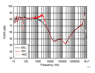
TPS657095 D001_SLVSCW2.gif
Figure 2. Power Supply Rejection Ratio (PSRR) for LDO1 at 1mA
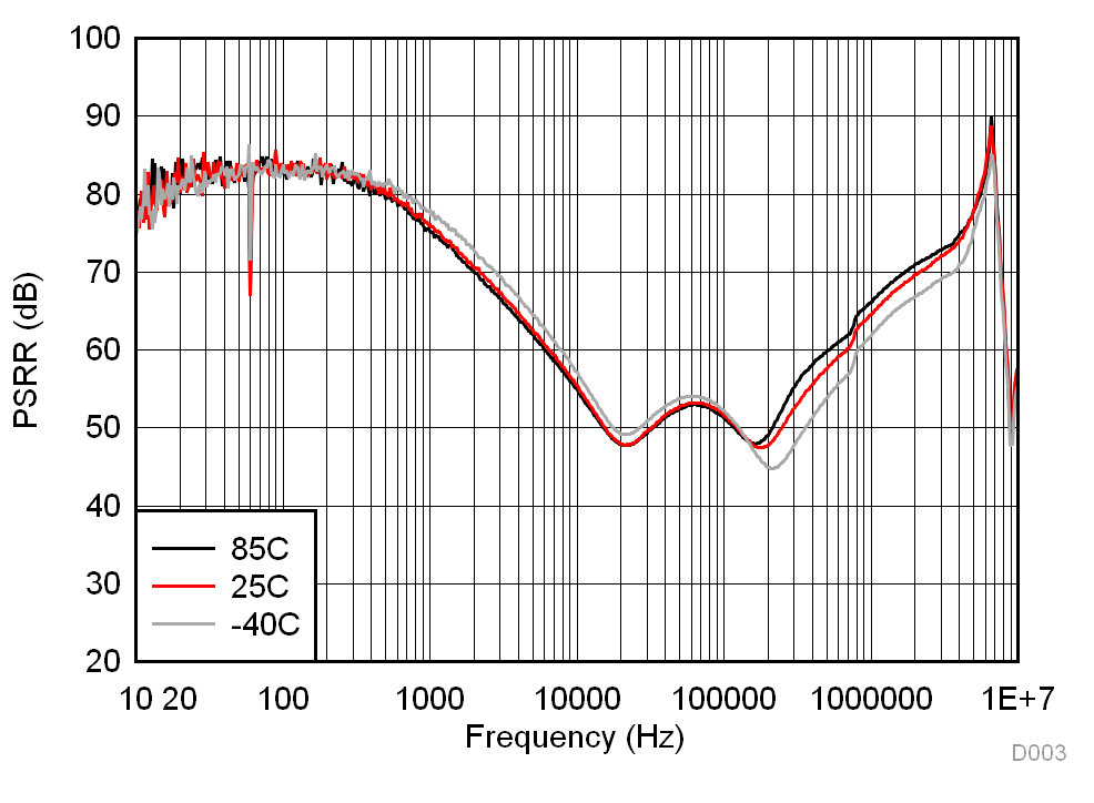
TPS657095 D003_SLVSCW2.gif
Figure 4. Power Supply Rejection Ratio (PSRR) for LDO2 at 1mA
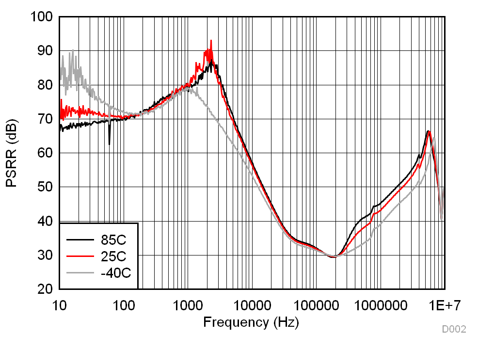
TPS657095 D002_SLVSCW2.gif
Figure 3. Power Supply Rejection Ratio (PSRR) for LDO1 at 75mA
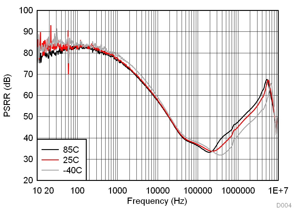
TPS657095 D004_SLVSCW2.gif
Figure 5. Power Supply Rejection Ratio (PSRR) for LDO2 at 75mA