SWCS048G March 2010 – September 2014 TPS65921
PRODUCTION DATA.
- 1Device Overview
- 2Revision History
- 3Terminal Configuration and Functions
-
4Specifications
- 4.1 Absolute Maximum Ratings
- 4.2 Handling Ratings
- 4.3 Recommended Operating Conditions
- 4.4 Thermal Resistance Characteristics for ZQZ Package
- 4.5 Crystal Oscillator
- 4.6 Clock Slicer
- 4.7 32KCLKOUT Output Clock
- 4.8 HFCLKOUT Output Clock
- 4.9 VDD1 DC-DC Converter
- 4.10 VDD2 DC-DC Converter
- 4.11 VIO DC-DC Converter
- 4.12 VMMC1 Low Dropout Regulator
- 4.13 VDAC Low Dropout Regulator
- 4.14 VAUX2 Low Dropout Regulator
- 4.15 VPLL1 Low Dropout Regulator
- 4.16 Internal LDOs
- 4.17 Voltage References
- 4.18 Battery Threshold Levels
- 4.19 Power Consumption
- 4.20 USB Charge Pump
- 4.21 Hot-Die Detection and Thermal Shutdown
- 4.22 USB
- 4.23 MADC
- 4.24 TPS65921 Interface Target Frequencies
- 4.25 JTAG Interfaces
- 5Detailed Description
- 6Device and Documentation Support
- 7Mechanical Packaging and Orderable Information
パッケージ・オプション
メカニカル・データ(パッケージ|ピン)
サーマルパッド・メカニカル・データ
発注情報
4 Specifications
4.1 Absolute Maximum Ratings(1)
over operating free-air temperature range (unless otherwise noted)| PARAMETER | TEST CONDITIONS | MIN | NOM | MAX | UNIT |
|---|---|---|---|---|---|
| Main battery supply voltage(2) | 0.0 | 5.0 | V | ||
| Voltage on any input(3) | Where supply represents the voltage applied to the power supply pin associated with the input(4) | –0.3 | 1.0 × Supply + 0.3 | V | |
| VBUS input | –0.3 | 7 | V | ||
| Operating ambient temperature (TA) | –40 | 85 | °C | ||
| Operating junction temperature (TJ) | Absolute maximum rating | –40 | 125 | °C | |
| Operating junction temperature (TJ) | For parametric compliance | –40 | 150 | °C | |
| Ambient temperature for parametric compliance | With maximum 125°C as junction temperature (TJ) | –40 | 85 | °C |
4.2 Handling Ratings
| MIN | MAX | UNIT | ||||
|---|---|---|---|---|---|---|
| Tstg | Storage temperature range | –55 | 125 | °C | ||
| VESD | Electrostatic discharge (ESD) performance: | Human Body Model (HBM), per ANSI/ESDA/JEDEC JS001(1) | –1 | 1 | kV | |
| Charged Device Model (CDM), per JESD22-C101(2) |
All pins | –250 | 250 | V | ||
4.3 Recommended Operating Conditions
over operating free-air temperature range (unless otherwise noted)| PARAMETER | MIN | TYP | MAX | UNIT | |||||
|---|---|---|---|---|---|---|---|---|---|
| Power and USB Path | |||||||||
| VBAT/VBAT.USB main battery supply voltage and | 2.7 | 3.6 | 4.5 | V | |||||
| VBUS | 0 | 7 | V | ||||||
| HFCLKIN Input Clock | |||||||||
| Frequency 1/tC(HFCLKIN) | 19.2, 26 or 38.4 | MHz | |||||||
| Pulse duration, HFCLKIN low or high (BP) | 0.45 × tC(HFCLKIN) | 0.55 × tC(HFCLKIN) | ns | ||||||
| HFCLKIN stability | –150 | 150 | ppm | ||||||
| Rise time of HFCLKIN (BP) | 0 | 5 | ns | ||||||
| Fall time of HFCLKIN (BP) | 0 | 5 | ns | ||||||
| Input dynamic range | LP/HP (sine wave) | 0.3 | 0.7 | 1.45 | Vpp | ||||
| BP/PD (square wave) | 0 | 1.85(1) | Vpp | ||||||
| Harmonic content of input signal (with 0.7-VPP amplitude): Second component - LP/HP (sine wave) | –25 | dBc | |||||||
| VIH voltage input high(1) | BP (square mode) | 0.65 × IO.1P8 | V | ||||||
| VIL voltage input low(1) | BP (square mode) | 0.35 × IO.1P8 | V | ||||||
| Crystal Oscillator | |||||||||
| Parallel resonance crystal frequency 1/tC(32KHZ) | 32.768 | kHz | |||||||
| Input voltage, Vin (normal mode) | 1.0 | 1.3 | 1.55 | V | |||||
| Crystal tolerance at room temperature, 25°C | –30 | 30 | ppm | ||||||
| Crystal tolerance versus temperature range (–40°C to 85°C) | –200 | 200 | ppm | ||||||
| Crystal quality factor | 13k | 54k | |||||||
| Maximum drive power | 1 | µW | |||||||
| Operating drive level | 0.5 | µW | |||||||
| 32KXIN 32KXOUT duty cycle |
Crystal | 40% | 60% | ||||||
| Square wave | 45% | 55% | |||||||
| 32-kHz clock rise/fall time | Square wave with capacitive load equivalent to 30 pF | 0.1 × tC(32KHZ) | µs | ||||||
| VIH voltage input high | Square wave in bypass mode(1) | 0.65 × VBRTC | V | ||||||
| VIL voltage input low | Square wave in bypass mode(1) | 0.35 × VBRTC | V | ||||||
| DC-DC Converters and LDOs | |||||||||
| VDD1.IN, VDD2.IN, VDD3.IN input voltage range for step-down converter VDD1, VDD2, VIO | 2.7 | 3.6 | 4.5 | V | |||||
| VMMC1.IN input voltage range for LDO VMMC1 | Maximum (2.7, output voltage selected + 250 mV) | 3.6 | 4.5 | V | |||||
| VDAC.IN input voltage range for LDO VDAC | 2.7 | 3.6 | 4.5 | V | |||||
| VAUX12S.IN input voltage range for LDO VAUX2 | Maximum (2.7, output voltage selected + 250 mV) | 3.6 | 4.5 | V | |||||
| VINT.IN input voltage range for LDO VINTANA1, VINTANA2, VINTDIG and VRTC | Maximum (2.7, output voltage selected + 200 mV) | 3.6 | 4.5 | V | |||||
| VPLLA3R.IN input voltage range for LDO VPLL1 | 2.7 | 3.6 | 4.5 | V | |||||
| VDD1.OUT ouput voltage range for VDD1 step-down converter | 0.6 | 1.45 | V | ||||||
| VDD2.OUT ouput voltage range for VDD2 step-down converter | 0.6 | 1.5 | V | ||||||
| VIO.OUT ouput voltage range for VIO step-down converter | 1.8/1.85 | V | |||||||
| VMMC1.OUT output voltage range for LDO VMMC1 | 1.85 | 3.15 | V | ||||||
| VDAC.OUT output voltage range for LDO VDAC | 1.2 | 1.8 | V | ||||||
| VAUX2.OUT output voltage range for LDO VAUX2 | 1.3 | 2.8 | V | ||||||
| VPLL1.OUT output voltage range for LDO VPLL1 | 1.0 | 1.8 | V | ||||||
| VINTANA1.OUT output voltage for LDO VINTANA1 | 1.5 | V | |||||||
| VINTANA2.OUT output voltage for LDO VINTANA2 | 2.5/2.75 | V | |||||||
| VINTUSB1P5V.OUT output voltage for LDO VINTUSB1P5 | 1.35 | 1.5 | 1.65 | V | |||||
| VINTUSB1P8V.OUT output voltage for LDO VINTUSB1P8 | 1.62 | 1.8 | 1.98 | V | |||||
| VUSB3P1V.OUT output voltage for LDO VUSB3P1 | 3.1 | V | |||||||
| VINTDIG.OUT output voltage range for LDO VINTDIG | 1.35 | 1.5 | 1.65 | V | |||||
| VRTC.OUT output voltage range | Normal mode | 1.45 | 1.5 | 1.55 | V | ||||
| Backup mode | 1.0 | 1.3 | 1.55 | V | |||||
| External Components | |||||||||
| Crystal: Nominal load cap on each oscillator input CXIN and CXOUT (2) | 9 | 10 | 12.5 | pF | |||||
| Crystal ESR (3) | 90 | kΩ | |||||||
| Crystal shunt capacitance, CO | 1 | pF | |||||||
| External coil for VDD1 | Value | 0.7 | 1 | 1.3 | µH | ||||
| DCR | 0.1 | Ω | |||||||
| Saturation current for TPS65921B | 1.8 | A | |||||||
| Saturation current for TPS65921B1 | 2.1 | A | |||||||
| External coil for VDD2 and VIO | Value | 0.7 | 1 | 1.3 | µH | ||||
| DCR | 0.1 | Ω | |||||||
| Saturation current | 900 | mA | |||||||
| External capacitor for VDD1, VDD2, VIO connected to VDD1.IN, VDD2.IN, VDD3.IN, and VDD1.OUT, VDD2.OUT, VIO.OUT | Value(4) | 5 | 10 | 15 | μF | ||||
| ESR at switching frequency | 1 | 20 | mΩ | ||||||
| Filtering capacitor for VMCC1.IN, VDAC.IN, VAUX12S.IN, VPPLA3R.IN, VINT.IN, VBAT.USB, VMMC1.OUT, VDAC.OUT, VAUX2.OUT, VPPL1, VINTDIG, VINTANA1, VINTANA2, VRRTC | Value | 0.3 | 1 | 2.7 | µF | ||||
| ESR | 20 | 600 | mΩ | ||||||
| Filtering capacitor for VUSB3V1, VUSB1V8, VUSB1V5 | Value | 0.5 | 2.2 | 6.5 | µF | ||||
| ESR | 20 | 600 | mΩ | ||||||
| Filtering capacitor for voltage reference | Connected from VREF to REFGND | 0.3 | 1 | 2.7 | µF | ||||
| External capacitor for charge pump and VBUS | Filtering capacitor (Connected between VBUS.CPOUT and GND) and called CVBUS | 1.41 (The minimum can be reduced to 1.2 µF, provided the charge-pump is only used to supply VUSB3V1 LDO) | 4.7 | 6.5 | µF | ||||
| Flying capacitor (Connected between CP.CAPP and CP.CAPM) called CVBUS.FC | 1.32 (The minimum can be reduced to 1.2 µF, provided the charge-pump is only used to supply VUSB3V1 LDO) | 2.2 | 3.08 | µF | |||||
| Filtering capacitor ESR for CVUSB.IN and CVBUS.FC | 20 | mΩ | |||||||
| Filtering capacitor CVBUS.IN | 5 | 10 | 15 | µF | |||||
| External capacitor for power reference filter | Filtering capacitor | 0.3 | 1 | 2.7 | µF | ||||
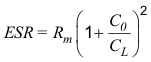
Measured with the load capacitance specified by the crystal manufacturer. In fact, if CXIN = CXOUT = 10 pF, then CL = 5 pF. Parasitic capacitance from the package and board must also be considered.
4.4 Thermal Resistance Characteristics for ZQZ Package
| NAME | DESCRIPTION | °C/W(1)(2) | AIR FLOW (m/s)(3) |
|---|---|---|---|
| RΘJC | Junction-to-case | 20 | 0.00 |
| RΘJB | Junction-to-board | 17 | 0.00 |
| RΘJA | Junction-to-free air | 46 | 0.00 |
| PsiJT | Junction-to-package top | 0.3 | 0.00 |
| PsiJB | Junction-to-board | 16 | 0.00 |
- JESD51-2, Integrated Circuits Thermal Test Method Environmental Conditions - Natural Convection (Still Air)
- JESD51-3, Low Effective Thermal Conductivity Test Board for Leaded Surface Mount Packages
- JESD51-7, High Effective Thermal Conductivity Test Board for Leaded Surface Mount Packages
- JESD51-9, Test Boards for Area Array Surface Mount Package Thermal Measurements
4.5 Crystal Oscillator
When selecting a crystal, the system designer must consider the temperature and aging characteristics of a crystal versus the user environment and expected lifetime of the system. The following table lists the switching characteristics of the oscillator.
Table 4-1 Base Oscillator Switching Characteristics
| PARAMETER | MIN | TYP | MAX | UNIT | ||
|---|---|---|---|---|---|---|
| Crystal: Internal capacitor on each input (Cint) | 8 | 10 | 12 | pF | ||
| Crystal: Parallel input capacitance (Cpin) | 1.0 | pF | ||||
| Parallel resonance crystal frequency | 32.768 | kHz | ||||
| Pin-to-pin capacitance | 1.6 | 1.8 | pF | |||
| Maximum drive power | 1.0 | µW | ||||
| Operating drive level | 0.5 | µW | ||||
| Crystal quality factor | 13k | 54k | ||||
| tSX | Start-up time, all conditions | 500 | ms | |||
| Start-up time, 25°C | 360 | |||||
| IDDA | Active current consumption (configured through the LOJIT bit) | High jitter mode | 1.8 | µA | ||
| Low jitter mode | 0.8 | |||||
| IDDQ | Current consumption | Low battery mode (1.2 V) | 1 | µA | ||
| Startup | 8 | |||||
4.6 Clock Slicer
| PARAMETER | MODE(1) | MIN | TYP | MAX | UNIT | |
|---|---|---|---|---|---|---|
| Internal coupling capacitor | 4.2 | 5 | 5.7 | pF | ||
| Parallel input resistance over 10 to 40 MHz range | LP | 15 | 60 | kΩ | ||
| HP | 30 | 75 | kΩ | |||
| BP/PD | 1 | 100 | MΩ | |||
| Parallel input capacitance over 10 to 40 MHz range | LP | 0.3 | 0.8 | pF | ||
| HP | 0.3 | 0.7 | ||||
| BP/PD | 0.08 | 1 | ||||
| BP/PD | 40 | 230 | ||||
| Output duty cycle with VIN = 0.2 VPP | LP/HP | 40% | 50% | 60% | ||
| Propagation delay | LP | 4 | 18 | ns | ||
| HP | 3 | 15 | ||||
| BP/PD | 0.2 | 3 | ||||
| Power supply rejection ratio sideband (1% RMS of supply voltage added sine 5 MHz) | LP/HP | 26 | dBc | |||
| Current consumption at maximum input of 40 MHz | LP | 175 | µA | |||
| HP | 235 | µA | ||||
| BP/PD | 39 | nA | ||||
| Power-up time | LP/HP | 1 | ms | |||
| Output peak-to-peak jitter with an input peak-to-peak jitter < 0.1% and for jitter frequency below 300 kHz | LP/HP | 0.2% | ||||
| Output peak-to-peak jitter with an input peak-to-peak jitter < 0.1% and for jitter frequency above 300 kHz | LP/HP | 1.0% | ||||
4.7 32KCLKOUT Output Clock
| NAME | PARAMETER DESCRIPTION | MIN | TYP | MAX | UNIT |
|---|---|---|---|---|---|
| f | Frequency | 32.768 | kHz | ||
| CL | Load capacitance | 40 | pF | ||
| VOUT | Output clock voltage, depending on output reference level IO.1P8 | 1.8(1) | V | ||
| VOH | Voltage output high | VOUT – 0.45 | VOUT | V | |
| VOL | Voltage output low | 0 | 0.45 | V |
The following table details the output clock timing characteristics. The following figure shows the 32KCLKOUT output clock waveform.
| NAME | PARAMETER | DESCRIPTION | MIN | TYP | MAX | UNIT |
|---|---|---|---|---|---|---|
| CK0 | 1/tC(32KCLKOUT) | Frequency | 32.768 | kHz | ||
| CK1 | tW(32KCLKOUT) | Pulse duration, 32KCLKOUT low or high | 0.40 × tC(32KCLKOUT) | 0.60 × tC(32KCLKOUT) | ns | |
| CK2 | tR(32KCLKOUT) | Rise time, 32KCLKOUT (1) | 16 | ns | ||
| CK3 | tF(32KCLKOUT) | Fall time, 32KCLKOUT (1) | 16 | ns | ||
| SSB Phase Noise | At 1-kHz offset from the carrier | –110 | dBc/Hz |
 Figure 4-1 32KCLKOUT Output Clock
4.8 HFCLKOUT Output Clock
The following table summarizes the HFCLKOUT output clock electrical characteristics.
Table 4-2 HFCLKOUT Output Clock Electrical Characteristics
| NAME | PARAMETER DESCRIPTION | MIN | TYP | MAX | UNIT |
|---|---|---|---|---|---|
| f | Frequency | 19.2, 26, or 38.4 | MHz | ||
| CL | Load capacitance | 30 | pF | ||
| VOUT | Output clock voltage, depending on output reference level IO.1P8 | 1.8(1) | V | ||
| VOH | Voltage output high | VOUT – 0.45 | VOUT | V | |
| VOL | Voltage output low | 0 | 0.45 | V | |
The following table details the HFCLKOUT output clock timing characteristics.
Table 4-3 HFCLKOUT Output Clock Switching Characteristics
| NAME | PARAMETER | DESCRIPTION | MIN | TYP | MAX | UNIT |
|---|---|---|---|---|---|---|
| CHO1 | 1/tC(HFCLKOUT) | Frequency | 19.2, 26, or 38.4 | MHz | ||
| CHO2 | tW(HFCLKOUT) | Pulse duration, HFCLKOUT low or high | 0.4 × tC(HFCLKOUT) | 0.6 × tC(HFCLKOUT) | ns | |
| CHO3 | tR(HFCLKOUT) | Rise time, HFCLKOUT, low drive(1) | ns | |||
| - Load: 5 pF | 3.8 | |||||
| - Load: 10 pF | 5.5 | |||||
| Rise time, HFCLKOUT, high drive(1) | ||||||
| - Load: 10 pF | 2.9 | |||||
| - Load: 20 pF | 5.0 | |||||
| CHO4 | tF(HFCLKOUT) | Fall time, HFCLKOUT, low drive(1) | ns | |||
| - Load: 5 pF | 3.5 | |||||
| - Load: 10 pF | 5.1 | |||||
| Fall time, HFCLKOUT, high drive(1) | ||||||
| - Load: 10 pF | 2.7 | |||||
| - Load: 20 pF | 4.7 | |||||
High drive: MISC_CFG[CLK_HF_DRV] = 1
Figure 4-2 shows the HFCLKOUT output clock waveform.
 Figure 4-2 HFCLKOUT Output Clock
Figure 4-3 shows the 32KCLKOUT and HFCLKOUT clock stabilization time.
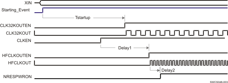
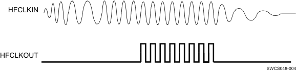 Figure 4-4 HFCLKOUT Behavior
4.9 VDD1 DC-DC Converter
| PARAMETER | COMMENTS | MIN | TYP | MAX | UNIT |
|---|---|---|---|---|---|
| Input voltage range | 2.7 | 3.6 | 4.5 | V | |
| Output voltage | 0.6 | 1.45 | V | ||
| Output voltage step | 0.6 to 1.45 V | 12.5 | mV | ||
| Output accuracy(1) | 0.6 to < 0.8 V | –6% | 6% | ||
| 0.8 to 1.45 V | –5% | 5% | |||
| Switching frequency | 3.2 | MHz | |||
| Conversion efficiency(2) | IO = 10 mA, sleep | 82% | |||
| 100 mA < IO < 400 mA | 85% | ||||
| 400 mA < IO < 600 mA | 80% | ||||
| 600 mA < IO < 800 mA | 75% | ||||
| Output current | Active mode Output voltage 0.6 V to 1.45 V for TPS65921B/TPS65921B1 |
1.2 | A | ||
| Active mode Output Voltage 1.2 V to 1.45 V for TPS65921B1 |
1.4 | A | |||
| Sleep mode | 10 | mA | |||
| Ground current (IQ) | Off at 30°C | 3 | µA | ||
| Sleep, unloaded | 30 | 50 | |||
| Active, unloaded, not switching | 300 | ||||
| Short-circuit current | VIN = VMAX | 2.2 | A | ||
| Load regulation | 0 < IO < IMAX | 20 | mV | ||
| Transient load regulation at 1.2 A(3) | IO = 10 mA to (IMAX/3) + 10 mA, maximum slew rate is IMAX/3/100 ns |
–65 | 50 | mV | |
| Line regulation | 10 | mV | |||
| Transient line regulation | 300 mVPP ac input, 10-μs rise and fall time | 10 | mV | ||
| Start-up time | 0.25 | 1 | ms | ||
| Recovery time | From sleep to on with constant load | < 10 | 100 | µs | |
| Slew rate (rising or falling)(4) | 4 | 8 | 16 | mV/µs | |
| Output ripple | Active (PWM and PSM) | –10 | 10 | mV | |
| Sleep (PFM) | –2% | 2% | |||
| Current limit for PWM/PSM mode switch. PSM is below this limit, and PWM is above this limit. | Active mode | 150 | 200 | mA | |
| Overshoot | Softstart | 5% | |||
| Output pulldown resistance | In Off mode | 500 | 700 | Ω |
4.10 VDD2 DC-DC Converter
| PARAMETER | COMMENTS | MIN | TYP | MAX | UNIT |
|---|---|---|---|---|---|
| Input voltage range | 2.7 | 3.6 | 4.5 | V | |
| Output voltage | 0.6 | 1.0 | 1.5 | V | |
| Output voltage step | 0.6 to 1.45 V | 12.5 | mV | ||
| Output accuracy(1) | 0.6 to < 0.8 V | –6% | 6% | ||
| 0.8 to 1.45 V | –5% | 5% | |||
| Switching frequency | 3.2 | MHz | |||
| Conversion efficiency(2) | IO = 10 mA, sleep | 82% | |||
| 100 mA < IO < 300 mA | 85% | ||||
| 300 mA < IO < 500 mA | 80% | ||||
| Output current | Active mode | 600 | mA | ||
| Sleep mode | 10 | mA | |||
| Ground current (IQ) | Off at 30°C | 1 | µA | ||
| Sleep, unloaded | 30 | 50 | |||
| Active, unloaded, not switching | 300 | ||||
| Short-circuit current | VIN = VMAX | 1.2 | A | ||
| Load regulation | 0 < IO < IMAX | 20 | mV | ||
| Transient load regulation(3) | IO = 10 mA to (IMAX/3) + 10 mA, maximum slew rate is IMAX/3/100 ns | –65 | 50 | mV | |
| Line regulation | 10 | mV | |||
| Transient line regulation | 300 mVPP ac input, 10-μs rise and fall time | 10 | mV | ||
| Output pulldown resistance | In OFF mode | 500 | 700 | Ω | |
| Start-up time | 0.25 | 1 | ms | ||
| Recovery time | From sleep to on with constant load | 25 | 100 | µs | |
| Slew rate (rising or falling)(4) | 4 | 8 | 16 | mV/µs | |
| Output ripple | Active (PWM and PSM) | –10 | 10 | mV | |
| Sleep (PFM) | –2% | 2% | |||
| Current limit for PWM/PSM mode switch. PSM is below this limit, and PWM is above this limit. | Active mode | 150 | 200 | mA | |
| Overshoot | Softstart | 5% |
4.11 VIO DC-DC Converter
| PARAMETER | COMMENTS | MIN | TYP | MAX | UNIT |
|---|---|---|---|---|---|
| Input voltage range | 2.7 | 3.6 | 4.5 | V | |
| Output voltage(1) | 1.8 1.85 |
V | |||
| Output accuracy | DC accuracy only | –3% | 3% | ||
| Including all variations (line and load regulations, line and load transients, temperature, and process) | –4% | 4% | |||
| Switching frequency | 3.2 | MHz | |||
| Conversion efficiency(2) | IO = 10 mA, sleep | 85% | |||
| 100 mA < IO < 400 mA | 85% | ||||
| 400 mA < IO < 600 mA | 80% | ||||
| Output current | On mode | 700 | mA | ||
| Sleep mode | 10 | mA | |||
| Ground current (IQ) | Off at 30°C | 1 | µA | ||
| Sleep, unloaded | 30 | 50 | |||
| Active, unloaded, not switching | 300 | ||||
| Load regulation | 0 < IO < IMAX | 20 | mV | ||
| Line regulation | 10 | mV | |||
| Transient load regulation | IO = 10 mA to (IMAX/3) + 10 mA, maximum slew rate is IMAX/3/100 ns | –65 | 50 | mV | |
| Transient line regulation | 300 mVPP ac input, 10-μs rise and fall time | 10 | mV | ||
| Start-up time | 0.25 | 1 | ms | ||
| Recovery time | From sleep to on with constant load | < 10 | 100 | µs | |
| Slew rate (rising or falling) | 4 | 8 | 16 | mV/µs | |
| Output ripple | Active (PWM and PSM) | –10 | 10 | mV | |
| Sleep (PFM) | –2% | 2% | |||
| Current limit for PWM/PSM mode switch. PSM is below this limit, and PWM is above this limit. | Active mode | 150 | 200 | mA | |
| Overshoot | Softstart | 5% | |||
| Output pulldown resistance | In Off mode | 500 | 700 | Ω |
4.12 VMMC1 Low Dropout Regulator
| PARAMETER | TEST CONDITIONS | MIN | TYP | MAX | UNIT | |
|---|---|---|---|---|---|---|
| VIN | Input voltage | 2.7 | 3.6 | 5.5 | V | |
| VOUT | Output voltage including all variations (line and load regulations, line and load transients, temperature, and process) | 1.7945 2.7645 2.91 3.0555 |
1.85 2.85 3.0 3.15 |
1.9055 2.9355 3.09 3.2445 |
V | |
| IOUT | Rated output current | On mode | 220 | mA | ||
| Low-power mode | 5 | |||||
| DC load regulation | On mode: 0 < IO < IMAX | 20 | mV | |||
| DC line regulation | On mode, VIN = VINmin to VINmax at IOUT = IOUTmax | 3 | mV | |||
| Turn-on time | IOUT = 0, CL = 1 μF (within 10% of VOUT) | 100 | µs | |||
| Wake-up time | Full load capability | 10 | µs | |||
| Ripple rejection | f < 10 kHz | 50 | dB | |||
| 10 kHz < f < 100 kHz | 40 | |||||
| f = 1 MHz | 25 | |||||
| VIN = VOUT + 1 V, IO = IMAX | ||||||
| Ground current | On mode, IOUT = 0 | 70 | µA | |||
| On mode, IOUT = IOUTmax | 290 | |||||
| Low-power mode, IOUT = 0 | 17 | |||||
| Low-power mode, IOUT = 5 mA | 20 | |||||
| Off mode at 55°C | 1 | |||||
| VDO | Dropout voltage(1) | On mode, IOUT = IOUTmax | 250 | mV | ||
| Transient load regulation(2) | ILOAD: IMIN – IMAX | –40 | 40 | mV | ||
| Slew: 40 mA/μs | ||||||
| Transient line regulation | VIN drops 500 mV | 10 | mV | |||
| Slew: 40 mV/μs | ||||||
| Overshoot | Softstart | 3% | ||||
| Pulldown resistance | Default in off mode | 250 | 320 | 450 | Ω | |
4.13 VDAC Low Dropout Regulator
| PARAMETER | TEST CONDITIONS | MIN | TYP | MAX | UNIT | |
|---|---|---|---|---|---|---|
| VIN | Input voltage | 2.7 | 3.6 | 4.5 | V | |
| VOUT | Output voltage including all variations (line and load regulations, line and load transients, temperature, and process) | 1.164 1.261 1.746 |
12 1.3 1.8 |
1.236 1.339 1.854 |
V | |
| IOUT | Rated output current | On mode | 70 | mA | ||
| Low-power mode | 5 | |||||
| DC load regulation | On mode: 0 < IO < IMAX | 20 | mV | |||
| DC line regulation | On mode, VIN = VINmin to VINmax at IOUT = IOUTmax | 3 | mV | |||
| Turn-on time | IOUT = 0, CL = 1 μF (within 10% of VOUT) | 100 | µs | |||
| Wake-up time | Full load capability | 10 | µs | |||
| Ripple rejection | f < 20 kHz | 65 | dB | |||
| 20 kHz < f < 100 kHz | 45 | |||||
| f = 1 MHz | 40 | |||||
| VIN = VOUT + 1 V, IO = IMAX | ||||||
| Output noise | 200 Hz < f < 5 kHz | 400 | nV/√Hz | |||
| 5 kHz < f < 400 kHz | 125 | |||||
| 400 kHz < f < 10 MHz | 50 | |||||
| Ground current | On mode, IOUT = 0 | 150 | µA | |||
| On mode, IOUT = IOUTmax | 350 | |||||
| Low-power mode, IOUT = 0 | 15 | |||||
| Low-power mode, IOUT = 1 mA | 25 | |||||
| Off mode at 55°C | 1 | |||||
| VDO | Dropout voltage(1) | On mode, IOUT = IOUTmax | 250 | mV | ||
| Transient load regulation(2) | ILOAD: IMIN – IMAX | –40 | 40 | mV | ||
| Slew: 60 mA/μs | ||||||
| Transient line regulation | VIN drops 500 mV | 10 | mV | |||
| Slew: 40 mV/μs | ||||||
| Overshoot | Softstart | 3% | ||||
| Pull down resistance | Default in off mode | 250 | 320 | 450 | Ω | |
4.14 VAUX2 Low Dropout Regulator
| PARAMETER | TEST CONDITIONS | MIN | TYP | MAX | UNIT | |
|---|---|---|---|---|---|---|
| VIN | Input voltage | 2.7 | 3.6 | 4.5 | V | |
| VOUT | Output voltage including all variations (line and load regulations, line and load transients, temperature, and process) | –3% | 1.3 1.5 1.7 1.8 1.9 2.0 2.1 2.2 2.3 2.4 2.5 2.8 |
+3% | V | |
| IOUT | Rated output current | On mode | 100 | mA | ||
| Low-power mode | 5 | |||||
| DC load regulation | On mode: 0 < IO < IMAX | 20 | mV | |||
| DC line regulation | On mode, VIN = VINmin to VINmax at IOUT = IOUTmax | 3 | mV | |||
| Turn-on time | IOUT = 0, CL = 1 μF (within 10% of VOUT) | 100 | µs | |||
| Wake-up time | Full load capability | 10 | µs | |||
| Ripple rejection | f < 10 kHz | 50 | dB | |||
| 10 kHz < f < 100 kHz | 40 | |||||
| f = 1 MHz | 30 | |||||
| VIN = VOUT + 1 V, IO = IMAX | ||||||
| Ground current | On mode, IOUT = 0 | 70 | µA | |||
| On mode, IOUT = IOUTmax | 170 | |||||
| Low-power mode, IOUT = 0 | 17 | |||||
| Low-power mode, IOUT = 5 mA | 20 | |||||
| Off mode at 55°C | 1 | |||||
| VDO | Dropout voltage(1) | On mode, IOUT = IOUTmax | 250 | mV | ||
| Transient load regulation(2) | ILOAD: IMIN – IMAX | –40 | 40 | mV | ||
| Slew: 40 mA/μs | ||||||
| Transient line regulation | VIN drops 500 mV | 10 | mV | |||
| Slew: 40 mV/μs | ||||||
| Overshoot | Softstart | 3% | ||||
| Pulldown resistance | Default in off mode | 250 | 320 | 450 | Ω | |
| Configurable as HighZ in off mode | 100 | MΩ | ||||
4.15 VPLL1 Low Dropout Regulator
| PARAMETER | TEST CONDITIONS | MIN | TYP | MAX | UNIT | |
|---|---|---|---|---|---|---|
| VIN | Input voltage | 2.7 | 3.6 | 4.5 | V | |
| VOUT | Output voltage including all variations (line and load regulations, line and load transients, temperature, and process) | 0.97 | 1.0 | 1.03 | V | |
| 1.164 | 1.2 | 1.236 | ||||
| 1.261 | 1.3 | 1.339 | ||||
| 1.746 | 1.8 | 1.854 | ||||
| IOUT | Rated output current | On mode | 40 | mA | ||
| Low-power mode | 5 | |||||
| DC load regulation | On mode: 0 < IO < IMAX | 20 | mV | |||
| DC line regulation | On mode, VIN = VINmin to VINmax at IOUT = IOUTmax | 3 | mV | |||
| Turn-on time | IOUT = 0, CL = 1 μF (within 10% of VOUT) | 100 | µs | |||
| Wake-up time | Full load capability | 10 | µs | |||
| Ripple rejection | f < 10 kHz | 50 | dB | |||
| 10 kHz < f < 100 kHz | 40 | |||||
| f = 1 MHz | 30 | |||||
| VIN = VOUT + 1 V, IO = IMAX | ||||||
| Ground current | On mode, IOUT = 0 | 70 | µA | |||
| On mode, IOUT = IOUTmax | 110 | |||||
| Low-power mode, IOUT = 0 | 15 | |||||
| Low-power mode, IOUT = 1 mA | 16 | |||||
| Off mode at 55°C | 1 | |||||
| VDO | Dropout voltage(1) | On mode, IOUT = IOUTmax | 250 | mV | ||
| Transient load regulation(2) | ILOAD: IMIN – IMAX | –40 | 40 | mV | ||
| Slew: 60 mA/μs | ||||||
| Transient line regulation | VIN drops 500 mV | 10 | mV | |||
| Slew: 40 mV/μs | ||||||
| Overshoot | Softstart | 3% | ||||
| Pulldown resistance | Default in off mode | 250 | 320 | 450 | Ω | |
4.16 Internal LDOs
Internal LDOs (except USBCP, which is a boost) are described in following table.
| NAME | USAGE | TYPE | VOLTAGE RANGE (V) | DEFAULT VOLTAGE (V) | MAXIMUM CURRENT |
|---|---|---|---|---|---|
| VINTANA1 | Internal | LDO | 1.5 | 1.5 | 50 mA |
| VINTANA2 | Internal | LDO | 2.5, 2.75 | 2.75 | 250 mA |
| VINTDIG | Internal | LDO | 1.5 | 1.5 | 100 mA |
| USBCP | Internal | Charge pump | 5 | 5 | 100 mA |
| VUSB1V5 | Internal | LDO | 1.5 | 1.5 | 30 mA |
| VUSB1V8 | Internal | LDO | 1.8 | 1.8 | 30 mA |
| VUSB3V1 | Internal | LDO | 3.1 | 3.1 | 14 mA |
| VRRTC | Internal | LDO | 1.5 | 1.5 | 30 mA |
| VBRTC | Internal | LDO | 1.3 | 1.3 | 100 μA |
4.17 Voltage References
| PARAMETER | TEST CONDITONS | MIN | TYP | MAX | UNIT |
|---|---|---|---|---|---|
| Internal bandgap reference voltage | On mode, measured through TESTV terminal | 1.272 | 1.285 | 1.298 | V |
| Reference voltage (VREF terminal) | On mode | 0.7425 | 0.75 | 0.7575 | V |
| Retention mode reference | On mode | 0.492 | 0.5 | 0.508 | V |
| IREF NMOS sink | 0.9 | 1.0 | 1.1 | µA | |
| Ground current | Bandgap | 25 | µA | ||
| IREF block | 20 | ||||
| Preregulator | 15 | ||||
| VREF buffer | 10 | ||||
| Retention reference buffer | 10 | ||||
| Output spot noise | 100 Hz | 1 | μV/√Hz | ||
| A-weighted noise (rms) | 200 | nV (rms) | |||
| P-weighted noise (rms) | 150 | nV (rms) | |||
| Integrated noise | 20 Hz to 100 kHz | 2.2 | µV | ||
| IBIAS trim bit LSB | 0.1 | µA | |||
| Ripple rejection | < 1 MHz from VBAT | 60 | dB | ||
| Start-up time | 1 | ms |
4.18 Battery Threshold Levels(1)
| PARAMETER | TEST CONDITIONS | MIN | TYP | MAX | UNIT |
|---|---|---|---|---|---|
| Main battery charged threshold VMBCH | Measured on VBAT terminal | 3.14 | 3.2 | 3.3 | V |
| Main battery low threshold VMBLO | Measured on VBAT terminal (monitored on terminal ONNOFF) | 2.55 | 2.7 | 2.8 | V |
| Main battery high threshold VMBHI | Measured on terminal VBAT | 2.5 | 2.65 | 3.0 | V |
| Batteries not present threshold VBNPR | Measured on terminal VBAT | 1.6 | 1.8 | 2.6 | V |
| Measured on terminal VBAT in slave mode | 1.95 | 2.1 | 2.6 | V |
4.19 Power Consumption
The typical power consumption is obtained in the nominal operating conditions and with the TPS65921 standalone.
| MODE | DESCRIPTION | TYPICAL CONSUMPTION | ||
|---|---|---|---|---|
| C021 boot mode | WAIT-ON | The phone is apparently off for the user, a main battery is present and well-charged. The RTC registers, registers in backup domain are maintained. The wakeup capabilities (like the PWRON button) are available. | VBAT = 3.8 V and Quartz present | 64 µA × 3.8 V = 243.2 μW |
| ACTIVE No Load HFCLK = 26 MHz | Subsystem is powered by the main battery. All supplies are enabled with no external load, internal reset is released, and the associated processor is running. USB interrupt handler consumes 433 µA (typ). | VBAT = 3.8 V | (2995 + 433) µA × 3.8 V = 13026 µW | |
| ACTIVE No Load HFCLK = 38.4 MHz | (3879 + 433) µA × 3.8 V = 16386 µW | |||
| SLEEP No Load | The main battery powers subsystem. Selected supplies are enabled but in low-consumption mode and associated processor is in low-power mode. | VBAT = 3.8 V | 492 µA × 3.8 V = 1870 µW | |
4.20 USB Charge Pump
| PARAMETER | TEST CONDITIONS | MIN | TYP | MAX | UNIT | |
|---|---|---|---|---|---|---|
| VIN | Input voltage | On mode: VIN = VBAT | 2.7 | 3.6 | 4.5 | V |
| VO | Output voltage | 4.625 | 5.0 | 5.25 | V | |
| Iload | Rated output current | VBAT > 3 V at VBUS | 0 | 100 | mA | |
| 2.7 V < VBAT < 3 V, at VBUS | 0 | 50 | ||||
| Efficiency | ILOAD = 100 mA, VBAT = 3.6 V | 55% | ||||
| Setting time | ILOADmax/2 to ILOADmax in 5 μs | 100 | 400 | µs | ||
| Start-up time | 3 | ms | ||||
| Short-circuit limitation current | 250 | 350 | 450 | mA | ||
| DC load regulation | ILOADmin to ILOADmax | 250 | 500 | mV | ||
| DC line regulation | 3.0 V to VBATmax | 250 | 350 | mV | ||
| ILOAD = 100 mA | ||||||
| Transient load regulation | IVBUS_5Vmax/2 – IVBUS_5Vmax | 300 | 350 | mV | ||
| 50 μs, C = 2 × 4.7 μF | ||||||
| 0 – IVBUS_5Vmax/2, 50 μs, C = 2 × 4.7 μF | 350 | |||||
| Transient line regulation | VBATmin to VBATmax in 50 μs, C = 2 × 4.7 μF | 300 | 350 | mV | ||
4.21 Hot-Die Detection and Thermal Shutdown
| PARAMETER | THRESHOLD (NOMINAL)(1) |
|---|---|
| Thermal hot-die selection THERM_HDSEL[1:0] | Threshold (nominal)(1) |
| 00 (1st hot-die threshold) | Rising temp: 120°C |
| Falling temp: 111°C | |
| 01 (2nd hot-die threshold) | Rising temp: 130°C |
| Falling temp: 121°C | |
| 10 (3rd hot-die threshold) | Rising temp: 140°C |
| Falling temp: 131°C | |
| 11 (4th hot-die threshold) | Not used |
| Thermal shutdown enable | Threshold (nominal)(1) - Rising temp: 150°C |
| Threshold (nominal)(1) - Falling temp: 140°C |
4.22 USB
4.22.1 LS/FS Single-Ended Receivers
| PARAMETER | COMMENTS | MIN | TYP | MAX | UNIT | |
|---|---|---|---|---|---|---|
| USB Single-Ended Receivers | ||||||
| Skew between VP and VM | SKWVP_VM | Driver outputs unloaded | –2 | 0 | 2 | ns |
| Single-ended hysteresis | VSE_HYS | 50 | mV | |||
| High (driven) | VIH | 2 | V | |||
| Low | VIL | 0.8 | V | |||
| Switching threshold | VTH | 0.8 | 2 | V | ||
4.22.2 LS/FS Differential Receiver
| PARAMETER | COMMENTS | MIN | TYP | MAX | UNIT | |
|---|---|---|---|---|---|---|
| Differential input sensitivity | VDI | Ref. USB2.0 | 200 | mV | ||
| Differential common mode range | VCM | Ref. USB2.0 | 0.8 | 2.5 | V | |
4.22.3 LS/FS Transmitter
| PARAMETER | COMMENTS | MIN | TYP | MAX | UNIT | |
|---|---|---|---|---|---|---|
| Low | VOL | Ref. USB2.0 | 0 | 300 | mV | |
| High (driven) | VOH | Ref. USB2.0 | 2.8 | 3.6 | V | |
| Output signal crossover voltage | VCRS | Ref. USB2.0, covered by eye diagram | 1.3 | 2.0 | V | |
| Rise time | TFR | Ref. USB2.0, covered by eye diagram | 75 | 300 | ns | |
| Fall time | TFF | 75 | 300 | ns | ||
| Differential rise and fall time matching | TFRFM | 80% | 125% | |||
| Low-speed data rate | TFDRATE | Ref. USB2.0, covered by eye diagram | 1.4775 | 1.5225 | Mbps | |
| Source jitter total (including frequency tolerance): | ||||||
| - To next transition | TDJ1 | Ref. USB2.0, covered by eye diagram | –25 | 25 | ns | |
| - For paired transitions | TDJ2 | –10 | 10 | |||
| Source SE0 interval of EOP | TFEOPT | Ref. USB2.0, covered by eye diagram | 1.25 | 1.5 | µs | |
| Downstream eye diagram | Ref. USB2.0, covered by eye diagram | |||||
| Differential common mode range | VCM | Ref. USB2.0 | 0.8 | 2.5 | V | |
4.22.4 FS Transmitter
| PARAMETER | COMMENTS | MIN | TYP | MAX | UNIT | |
|---|---|---|---|---|---|---|
| Low | VOL | Ref. USB2.0 | 0 | 300 | mV | |
| High (driven) | VOH | Ref. USB2.0 | 2.8 | 3.6 | V | |
| Output signal crossover voltage | VCRS | Ref. USB2.0, covered by eye diagram | 1.3 | 2.0 | V | |
| Rise time | TFR | Ref. USB2.0 | 4 | 20 | ns | |
| Fall time | TFF | Ref. USB2.0 | 4 | 20 | ns | |
| Differential rise and fall time matching | TFRFM | Ref. USB2.0, covered by eye diagram | 90% | 111.11% | ||
| Driver output resistance | ZDRV | Ref. USB2.0 | 28 | 44 | Ω | |
| Full-speed data rate | TFDRATE | Ref. USB2.0, covered by eye diagram | 11.97 | 12.03 | Mbps | |
| Source jitter total (including frequency tolerance): | ||||||
| - To next transition | TDJ1 | Ref. USB2.0, covered by eye diagram | –2 | 2 | ns | |
| - For paired transitions | TDJ2 | –1 | 1 | |||
| Source SE0 interval of EOP | TFEOPT | Ref. USB2.0, covered by eye diagram | 160 | 175 | ns | |
| Downstream eye diagram | Ref. USB2.0, covered by eye diagram | |||||
| Upstream eye diagram | ||||||
4.22.5 HS Differential Receiver
| PARAMETER | COMMENTS | MIN | TYP | MAX | UNIT | |
|---|---|---|---|---|---|---|
| High-speed squelch detection threshold (differential signal amplitude) | VHSSQ | Ref. USB2.0 | 100 | 150 | mV | |
| High-speed disconnect detection threshold (differential signal amplitude) | VHSDSC | Ref. USB2.0 | 525 | 625 | V | |
| High-speed differential input signaling levels | Ref. USB2.0, specified by eye pattern templates | mV | ||||
| High-speed data signaling common mode voltage range (guidelines for receiver) | VHSCM | Ref. USB2.0 | –50 | 600 | mV | |
| Receiver jitter tolerance | Ref. USB2.0, specified by eye pattern templates | 150 | ps | |||
4.22.6 HS Transmitter
| PARAMETER | COMMENTS | MIN | TYP | MAX | UNIT | |
|---|---|---|---|---|---|---|
| High-speed idle level | VHSOI | Ref. USB2.0 | –10 | 10 | mV | |
| High-speed data signaling high | VHSOH | Ref. USB2.0 | 360 | 440 | mV | |
| High-speed data signaling low | VHSOL | Ref. USB2.0 | –10 | 10 | mV | |
| Chirp J level (differential voltage) | VCHIRPJ | Ref. USB2.0 | 700 | 1100 | mV | |
| Chirp K level (differential voltage) | VCHIRPK | Ref. USB2.0 | –825 | –500 | mV | |
| Rise Time (10% – 90%) | THSR | Ref. USB2.0, covered by eye diagram | 500 | |||
| Fall time (10% – 90%) | THSR | Ref. USB2.0, covered by eye diagram | 500 | |||
| Driver output resistance (which also serves as high-speed termination) | ZHSDRV | Ref. USB2.0 | 40.5 | 49.5 | Ω | |
| High-speed data range | THSDRAT | Ref. USB2.0, covered by eye diagram | 479.76 | 480.24 | Mbps | |
| Data source jitter | Ref. USB2.0, covered by eye diagram | |||||
| Downstream eye diagram | Ref. USB2.0, covered by eye diagram | |||||
| Upstream eye diagram | Ref. USB2.0, covered by eye diagram | |||||
4.22.7 UART Transceiver
| PARAMETER | MIN | MAX | UNIT | |
|---|---|---|---|---|
| tPH_DP_CON | Phone D+ connect time | 100 | ms | |
| tPH_DISC_DET | Phone D+ disconnect time | 150 | ms | |
| fUART_DFLT | Default UART signaling rate (typical rate) | 9600 | bps | |
| PARAMETER | COMMENTS | MIN | TYP | MAX | UNIT | |
|---|---|---|---|---|---|---|
| UART Transmitter CEA-2011 | ||||||
| Phone UART edge rates | tPH_UART_EDGE | DP_PULLDOWN asserted | 1 | ms | ||
| Serial interface output high | VOH_SER | ISOURCE = 4 mA | 2.4 | 3.3 | 3.6 | V |
| Serial interface output low | VOL_SER | ISINK = –4 mA | 0 | 0.1 | 0.4 | V |
| UART Receiver CEA-2011 | ||||||
| Serial interface input high | VIH_SER | DP_PULLDOWN asserted | 2.0 | V | ||
| Serial interface input low | VIL_SER | DP_PULLDOWN asserted | 0.8 | V | ||
| Switching threshold | VTH | 0.8 | 2.0 | V | ||
4.22.8 Pullup/Pulldown Resistors
| PARAMETER | COMMENTS | MIN | TYP | MAX | UNIT | |
|---|---|---|---|---|---|---|
| Pullup Resistors | ||||||
| Bus pullup resistor on upstream port (idle bus) | RPUI | Bus idle | 0.9 | 1.1 | 1.575 | kΩ |
| Bus pullup resistor on upstream port (receiving) | RPUA | Bus driven/driver's outputs unloaded | 1.425 | 2.2 | 3.09 | |
| High (floating) | VIHZ | Pullups/pulldowns on both DP and DM lines | 2.7 | 3.6 | V | |
| Phone D+ pullup voltage | VPH_DP_UP | Driver's outputs unloaded | 3.0 | 3.3 | 3.6 | V |
| Pulldown Resistors | ||||||
| Phone D+/– pulldown | RPH_DP_DWN | Driver's outputs unloaded | 14.25 | 18 | 24.8 | kΩ |
| RPH_DM_DWN | ||||||
| High (floating) | VIHZ | Pullups/pulldowns on both DP and DM lines | 2.7 | 3.6 | V | |
| D+/– Data line | ||||||
| Upstream facing port | CINUB | [1.0] | 22 | 75 | pF | |
| On-the-go device leakage | VOTG_DATA_LKG | [2] | 0.342 | V | ||
| Input impedance exclusive of pullup/pulldown | ZINP | Driver’s outputs unloaded | 300 | kΩ | ||
4.22.9 OTG VBUS
| PARAMETER | COMMENTS | MIN | TYP | MAX | UNIT | |
|---|---|---|---|---|---|---|
| VBUS Wakeup Comparator | ||||||
| VBUS wake-up delay | DELVBUS_WK_UP | 15 | µs | |||
| VBUS Comparators | ||||||
| A-device session valid | VA_SESS_VLD | 0.8 | 1.1 | 1.4 | V | |
| A-device VBUS valid | VA_VBUS_VLD | 4.4 | 4.5 | 4.625 | V | |
| B-device session end | VB_SESS_END | 0.2 | 0.5 | 0.8 | V | |
| B-device session valid | VB_SESS_VLD | 2.1 | 2.4 | 2.7 | V | |
| VBUS Line | ||||||
| A-device VBUS input impedance to ground | RA_BUS_IN | SRP (VBUS pulsing) capable A-device not driving VBUS | 13.77 | 100 | kΩ | |
| B-device VBUS SRP pulldown | RB_SRP_DWN | 5.25 V / 8 mA, pullup voltage = 3 V | 0.656 | 10 | kΩ | |
| B-device VBUS SRP pullup | RB_SRP_UP | (5.25 V – 3 V) / 8 mA, pullup voltage = 3 V | 0.85 | 1.3 | 1.75 | kΩ |
| B-device VBUS SRP rise time maximum for OTG-A communication | tRISE_SRP_UP_MAX | 0 to 2.1 V with < 13 μF load | 34 | ms | ||
| B-device VBUS SRP rise time minimum for standard host connection | tRISE_SRP_UP_MIN | 0.8 to 2.0 V with > 97 μF load | 46 | ms | ||
4.22.10 OTG ID
| PARAMETER | COMMENTS | MIN | TYP | MAX | UNIT | |
|---|---|---|---|---|---|---|
| VBUS Wakeup Comparator | ||||||
| ID wake-up comparator | RID_WK_UP | Wakeup when ID shorted to ground. | 30 | 100 | kΩ | |
| ID Comparators — ID External Resistors Specifications | ||||||
| ID ground comparator | RID_GND | ID_GND interrupt | 4 | 20 | 25 | kΩ |
| ID Float comparator | RID_FLOAT | ID_FLOAT interrupt | 200 | 500 | kΩ | |
| ID Line | ||||||
| Phone ID pullup to VPH_ID_UP | RPH_ID_UP | ID unloaded (VRUSB) | 70 | 90 | 286 | kΩ |
| Phone ID pullup voltage | VPH_ID_UP | Connected to VRUSB | 2.5 | 3.2 | V | |
| ID line maximum voltage | 5.25 | V | ||||
4.22.11 USB Charger Detection
| USB Charger Detection Debounce Time | |||||||
|---|---|---|---|---|---|---|---|
| REQUIREMENT | PARAMETER | NB CLOCK | TEST CONDITIONS | MIN | TYP | MAX | UNIT |
| Minimum 10 ms | DEBVBUS_TIME | 448 | ACTIVE/SLEEP mode | 13.7 | 13.7 | ms | |
| Minimum 20 ms | DEBUSBCHG_TIME | 896 | ACTIVE/SLEEP mode | 27.3 | 27.3 | ms | |
Table 4-4 Voltages
| PARAMETER | SYMBOL | CONDITIONS | MIN | MAX | UNIT | REF |
|---|---|---|---|---|---|---|
| Logic Threshold | VLGC | 0.8 | 2.0 | V | 1.4.4 | |
| D+ Source Voltage | VDP_SRC | Output current > 250 µA | 0.5 | 0.675 | V | |
| Data Detect Voltage | VDAT_REF | 0.25 | 0.4 | V | ||
| Data Line Leakage Voltage | VDAT_LKG | 0 | 3.6 | V | 3.9 |
Table 4-5 Currents
| PARAMETER | SYMBOL | CONDITIONS | MIN | MAX | UNIT | REF |
|---|---|---|---|---|---|---|
| Portable Device Current from Charging Host Port during chirp | IDEV_HCHG_CHRP | 710 | mA | 3.6.2 | ||
| Data Contact Detect Current Source | IDP_SRC | 7 | 13 | µA | ||
| D- Sink Current | IDM_SINK | 50 | 150 | µA |
Table 4-6 Resistances
| PARAMETER | SYMBOL | CONDITIONS | MIN | MAX | UNIT |
|---|---|---|---|---|---|
| D+ pulldown resistance | RDP_DWN | 14.25 | 24.8 | kΩ | |
| D- pulldown resistance | RDM_DWN | 14.25 | 24.8 | kΩ |
Table 4-7 USB Charger Detection (Wait and Debounce Timing)
| USB Charger Detection (Wait and Debounce Timing) | |||||||
|---|---|---|---|---|---|---|---|
| Requirement | PARAMETER | NB CLOCK | TEST CONDITIONS | MIN | TYP | MAX | UNIT |
| Minimum 200 us | D+ Current source on-time TIDP_SRC_ON |
8 | ACTIVE/SLEEP mode(1) | 244.1 | 244.1 | µs | |
| Minimum 40 ms | D+ Voltage source on-time TVDP_SRC_ON |
1792 | ACTIVE/SLEEP mode(1) | 54.7 | 54.7 | ms | |
| Minimum 40 ms | D+ Voltage source off to high current TVDP_SRC_HICRNT |
1792 | ACTIVE/SLEEP mode(1) | 54.7 | 54.7 | ms | |
| Minimum 2 s | DATA_CONTACT_DETECT Timeout TDCD_TIMEOUT |
89600 | ACTIVE/SLEEP mode(1) | 2.73 | 2.73 | s | |
4.23 MADC
| PARAMETER | CONDITIONS | MIN | TYP | MAX | UNIT |
|---|---|---|---|---|---|
| Resolution | 10 | Bit | |||
| Input dynamic range for external input ADCIN0 | 0 | 1.5 | V | ||
| MADC voltage reference | 1.5 | V | |||
| Differential nonlinearity | –1 | 1 | LSB | ||
| Integral nonlinearity | Best fitting | –2 | 2 | LSB | |
| Offset | Best fitting | –28.5 | 28.5 | mV | |
| Input bias | 1 | μA | |||
| Input capacitor CBANK | 10 | pF | |||
| Input current leakage | 1 | μA |
4.23.1 MADC Analog Input Range and Prescaler Ratio
| MADC CHANNEL | INT/EXT | ANALOG INPUT RANGE (V) | PRESCALER | ||||
|---|---|---|---|---|---|---|---|
| MIN | MAX | OUTPUT RANGE (V) | DIVIDER RATIO | NOTE | |||
| MIN | MAX | ||||||
| ADCIN0: General-purpose input (1) | External | 0.0 | 1.5 | N/A | N/A | 1 | No prescaler |
| ADCIN1:7 Reserved | Internal | N/A | N/A | N/A | N/A | N/A | Not used |
| ADCIN8: VBUS Voltage (VBUS) | Internal | 0.0 | 6.5 | 0.0 | 1.5 | 3/14 | Prescaler in USB subchip. |
| Rdivider = (6 × 2.76 kΩ)/(28 × 2.76 kΩ) (typ)(3) | |||||||
| ADCIN9: Reserved | Internal | Not used | |||||
| ADCIN10:11 Reserved | Internal | N/A | N/A | N/A | N/A | N/A | |
| ADCIN12: Main battery voltage (VBAT) | Internal | 2.7 | 4.7 | 0.675 | 1.175 | 0.25 | Prescaler integrated |
| Rdivider = 9.85 kΩ/(4 × 9.85 kΩ) (typ)(2) | |||||||
| ADCIN13:15 Reserved | Internal | N/A | N/A | N/A | N/A | N/A | |
The table below summarizes the sequence conversion timing characteristics. Figure 4-5 shows one conversion sequence general timing diagram.
Table 4-8 Sequence Conversion Timing Characteristics
| PARAMETER | COMMENTS | MIN | TYP | MAX | UNIT |
|---|---|---|---|---|---|
| F | Running frequency | 1 | MHz | ||
| T = 1/F | Clock period | 1 | μs | ||
| N | Number of analog inputs to convert in a single sequence | 0 | 16 | ||
| Tstart | SW1, SW2, or USB asynchronous request or real-time STARTADC request | 3 | 4 | μs | |
| Tsettling time | Settling time to wait before sampling a stable analog input (capacitor bank charge time) | 5 | 12 | 260 | μs |
| Tsettling is calculated from the max((Rs + Ron)*Cbank) of all possible input sources (internal or external). Ron is the resistance of the selection analog input switches (5 kΩ). This time is software programmable by OCP register; default value is 12 µs. | |||||
| Tstartsar | The successive approximation registers ADC start time | 1 | μs | ||
| Tadc time | The successive approximation registers ADC conversion time | 10 | μs | ||
| Tcapture time | Tcapture time is the conversion result capture time. | 2 | μs | ||
| Tstop | 1 | 2 | μs | ||
| Full Conversion Sequence Time | Only one channel (N = 1) (1) | 22 | 39 | μs | |
| All channels(2) | 352 | 624 | |||
| Conversion Sequence Time | Without Tstart and Tstop: Only one channel (N = 1) (1) | 18 | 33 | μs | |
| Without Tstart and Tstop: All channels(1) | 288 | 528 | |||
| STARTADC pulse duration | STARTADC period is T | 0.33 | μs |
This table is illustrated in Figure 4-5. The Busy parameter indicates that a conversion sequence is running, and the channel N result register parameter corresponds to the result register of RT/GP selected channel.
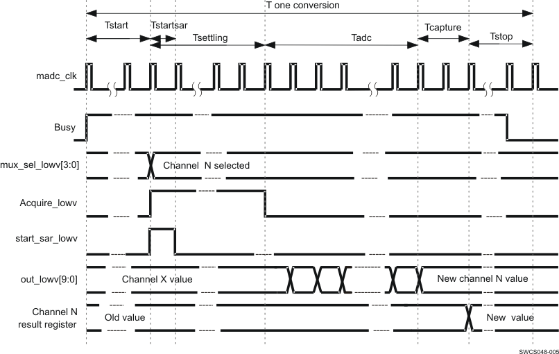 Figure 4-5 One Conversion Sequence General Timing Diagram
4.23.2 MADC Power Consumption
| PARAMETER | TEST CONDITIONS | MIN | TYP | MAX | UNIT |
|---|---|---|---|---|---|
| Power on consumption | Running frequency f = 1 MHz | 1(1) | mA | ||
| Power down consumption | 1 | μA |
4.24 TPS65921 Interface Target Frequencies
Table below assumes testing over the recommended operating conditions.
| I/O INTERFACE | INTERFACE DESIGNATION | TARGET FREQUENCY | |
|---|---|---|---|
| 1.5 V | |||
| SmartReflex I2C | Slave high-speed mode | 3.6 Mbps | |
| General-purpose I2C | I2C Interface | Slave fast-speed mode | 400 kbps |
| Slave standard mode | 100 kbps | ||
| High speed | 480 Mbps | ||
| USB | USB | Full speed | 12 Mbps |
| Low speed | 1.5 Mbps | ||
| Real/View® ICE tool | 30 MHz | ||
| JTAG | XDS560 and XDS510 tools | 30 MHz | |
| Lauterbach™ tool | 30 MHz | ||
4.24.1 I2C Timing
The TPS65921 provides two I2C HS slave interfaces (one for general-purpose and one for SmartReflex). These interfaces support the standard mode (100 kbps), fast mode (400 kbps), and HS mode (3.5 Mbps). The general-purpose I2C module embeds four different slave hard-coded addresses (ID1 = 48h, ID2 = 49h, ID3 = 4Ah, and ID4 = 4Bh). The SmartReflex I2C module uses one slave hard-coded address (ID5). The master mode is not supported.
Table 4-9 and Table 4-10 assume testing over the recommended operating conditions.
 Figure 4-6 I2C Interface—Transmit and Receive in Slave Mode
Table 4-9 I2C Interface Timing Requirements(1)(2)
| NO. | PARAMETER | MIN | MAX | UNIT | |
|---|---|---|---|---|---|
| Slave High-Speed Mode | |||||
| I3 | tsu(SDA-SCLH) | Setup time, SDA valid to SCL high | 10 | ns | |
| I4 | th(SCLL-SDA) | Hold time, SDA valid from SCL low | 0 | 70 | ns |
| I7 | tsu(SCLH-SDAL) | Setup time, SCL high to SDA low | 160 | ns | |
| I8 | th(SDAL-SCLL) | Hold time, SCL low from SDA low | 160 | ns | |
| I9 | tsu(SDAH-SCLH) | Setup time, SDA high to SCL high | 160 | ns | |
| Slave Fast-Speed Mode | |||||
| I3 | tsu(SDA-SCLH) | Setup time, SDA valid to SCL high | 100 | ns | |
| I4 | th(SCLL-SDA) | Hold time, SDA valid from SCL low | 0 | 0.9 | µs |
| I7 | tsu(SCLH-SDAL) | Setup time, SCL high to SDA low | 0.6 | µs | |
| I8 | th(SDAL-SCLL) | Hold time, SCL low from SDA low | 0.6 | µs | |
| I9 | tsu(SDAH-SCLH) | Setup time, SDA high to SCL high | 0.6 | µs | |
| Slave Standard Mode | |||||
| I3 | tsu(SDA-SCLH) | Setup time, SDA valid to SCL high | 250 | ns | |
| I4 | th(SCLL-SDA) | Hold time, SDA valid from SCL low | 0 | ns | |
| I7 | tsu(SCLH-SDAL) | Setup time, SCL high to SDA low | 4.7 | µs | |
| I8 | th(SDAL-SCLL) | Hold time, SCL low from SDA low | 4 | µs | |
| I9 | tsu(SDAH-SCLH) | Setup time, SDA high to SCL high | 4 | µs | |
80 ns in high-speed mode (3.4 Mbits/s)
300 ns in fast-speed mode (400 Kbits/s)
1000 ns in standard mode (100 Kbits/s)
SCL is equal to I2C.SR.SCL or I2C.CNTL.SCL
Table 4-10 I2C Interface Switching Requirements(1)(2)
| NO. | PARAMETER | MIN | MAX | UNIT | |
|---|---|---|---|---|---|
| Slave High-speed Mode | |||||
| I1 | tw(SCLL) | Pulse duration, SCL low | 160 | ns | |
| I2 | tw(SCLH) | Pulse duration, SCL high | 60 | ns | |
| Slave Fast-speed Mode | |||||
| I1 | tw(SCLL) | Pulse duration, SCL low | 1.3 | µs | |
| I2 | tw(SCLH) | Pulse duration, SCL high | 0.6 | µs | |
| Slave Standard Mode | |||||
| I1 | tw(SCLL) | Pulse duration, SCL low | 4.7 | µs | |
| I2 | tw(SCLH) | Pulse duration, SCL high | 4 | µs | |
100 pF in high-speed mode (3.4 Mbits/s)
400 pF in fast-speed mode (400 Kbits/s)
400 pF in standard mode (100 Kbits/s)
SCL is equal to I2C.SR.SCL or I2C.CNTL.SCL
4.25 JTAG Interfaces
Table 4-11 and Table 4-12 assume testing over the recommended operating conditions.
 Figure 4-7 JTAG Interface Timing
The input timing requirements are given by considering a rising or falling edge of 7 ns.
4.25.1 JTAG Interface Timing Requirements
Table 4-11 JTAG Interface Timing Requirements
| NO. | PARAMETER | MIN | MAX | UNIT | |
|---|---|---|---|---|---|
| Clock | |||||
| JL1 | tc(TCK) | Cycle time, JTAG.TCK period | 30 | ns | |
| JL2 | tw(TCK) | Pulse duration, JTAG.TCK high or low (1) | 0.48 × P | 0.52 × P | ns |
| Read Timing | |||||
| JL3 | tsu(TDIV-TCKH) | Setup time, JTAG.TDI valid before JTAG.TCK high | 8 | ns | |
| JL4 | th(TDIV-TCKH) | Hold time, JTAG.TDI valid after JTAG.TCK high | 5 | ns | |
| JL5 | tsu(TMSV-TCKH) | Setup time, JTAG.TMS valid before JTAG.TCK high | 8 | ns | |
| JL6 | th(TMSV-TCKH) | Hold time, JTAG.TMS valid after JTAG.TCK high | 5 | ns | |
The capacitive load is equivalent to 35 pF.
4.25.2 JTAG Interface Switching Characteristics
Table 4-12 JTAG Interface Switching Characteristics
| NO. | PARAMETER | MIN | MAX | UNIT | |
|---|---|---|---|---|---|
| Write Timing | |||||
| JL7 | td(TCK-TDOV)) | Delay time, JTAG, TCK active edge to JTAG.TDO valid | 0 | 14 | ns |
| NO. | PARAMETER | MIN | MAX | UNIT | |
| Clock | |||||
| JL1 | tc(TCK) | Cycle time, JTAG.TCK period | 30 | ns | |
| JL2 | tw(TCK) | Pulse duration, JTAG.TCK high or low(1) | 0.48 × P | 0.52 × P | ns |
| Read Timing | |||||
| JL3 | tsu(TDIV-TCKH) | Setup time, JTAG.TDI valid before JTAG.TCK high | 8 | ns | |
| JL4 | th(TDIV-TCKH) | Hold time, JTAG.TDI valid after JTAG.TCK high | 5 | ns | |
| JL5 | tsu(TMSV-TCKH) | Setup time, JTAG.TMS valid before JTAG.TCK high | 8 | ns | |
| JL6 | th(TMSV-TCKH) | Hold time, JTAG.TMS valid after JTAG.TCK high | 5 | ns | |
4.25.3 Debouncing Time
Debounce times are listed in Table 4-13.
Table 4-13 Debouncing Time
| DEBOUNCING FUNCTIONS | BLOCK | PROGRAMMABLE | DEBOUNCING TIME | DEFAULT |
|---|---|---|---|---|
| Main battery charged threshold (<3.2 V) | Battery monitoring | No | 580 μs | 580 μs |
| Main battery low threshold detection (<2.7 V) | No | 60 μs | 60 μs | |
| Main battery plug detection | No | 60 μs | 60 μs | |
| Debouncing functions interrupt generation debounce | POWER | No | 125.6 μs | 125.6 μs |
| Plug/unplug detection VBUS (1) | USB | Yes | 0 to 250 ms (32/32768-second stgif) |
30 ms |
| Plug/unplug detection ID(2) | USB | Yes | 0 to 250 ms (32/32768-second stgif) |
50 ms |
| Debouncing functions interrupt generation debounce for VBUS and ID(3) | POWER | Yes | 0 to 233 ms | 28 ms |
| Hot-die detection | Thermistor | No | 60 μs | 60 μs |
| Thermal shutdown detection | No | 60 μs | 60 μs | |
| PWRON(4) | Start/stop button | No | 31.25 ms | 31.25 ms |
| NRESWARM | Button reset | No | 60 μs | 60 μs |
| MMC1/2 (plug/unplug) | GPIO | Yes | 0 or 28 ms ± 2 ms | 0 ms |