JAJSEP4C June 2018 – May 2022 TPS746-Q1
PRODUCTION DATA
- 1 特長
- 2 アプリケーション
- 3 概要
- 4 Revision History
- 5 Pin Configuration and Functions
- 6 Specifications
- 7 Detailed Description
- 8 Application and Implementation
- 9 Power Supply Recommendations
- 10Layout
- 11Device and Documentation Support
パッケージ・オプション
メカニカル・データ(パッケージ|ピン)
サーマルパッド・メカニカル・データ
発注情報
8.2.2.1 Input Current
During normal operation, the input current to the LDO is approximately equal to the output current of the LDO. During startup, the input current is higher as a result of the inrush current charging the output capacitor. Use Equation 6 to calculate the current through the input.
Equation 6. 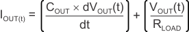
where:
- VOUT(t) is the instantaneous output voltage of the turn-on ramp
- dVOUT(t) / dt is the slope of the VOUT ramp
- RLOAD is the resistive load impedance