JAJS401H november 2007 – april 2023 TPS74701
PRODUCTION DATA
- 1
- 1 特長
- 2 アプリケーション
- 3 概要
- 4 Revision History
- 5 Pin Configuration and Functions
-
6 Specifications
- 6.1 Absolute Maximum Ratings
- 6.2 ESD Ratings
- 6.3 Recommended Operating Conditions
- 6.4 Thermal Information
- 6.5 Electrical Characteristics: Other Orderable Devices (non-M3 Suffix)
- 6.6 Electrical Characteristics: Orderable Device (M3 Suffix)
- 6.7 Typical Characteristics: VEN = VIN (All Other Orderable Devices, Non-M3 Suffix)
- 6.8 Typical Characteristics: VEN = VIN = 1.8 V, VOUT = 1.5 V (All Other Orderable Devices, Non-M3 Suffix)
- 6.9 Typical Characteristics: IOUT = 50 mA (M3 Suffix)
- 6.10 Typical Characteristics: VEN = VIN = 1.8 V, VOUT = 1.5 V (M3 Suffix)
- 7 Detailed Description
- 8 Application and Implementation
- 9 Device and Documentation Support
- 10Mechanical, Packaging, and Orderable Information
パッケージ・オプション
メカニカル・データ(パッケージ|ピン)
- DRC|10
サーマルパッド・メカニカル・データ
- DRC|10
発注情報
8.1 Application Information
R1 and R2 can be calculated for any output voltage using the formula in Figure 8-4. Table 8-1 lists sample resistor values of common output voltages. To achieve the maximum accuracy specifications, R2 must be less than or equal to 4.99 kΩ. Table 8-2 lists the capacitor values for setting the soft-start time.
Table 8-1 Standard 1% Resistor Values
for Programming the Output Voltage(1)
| R1 (kΩ) | R2 (kΩ) | VOUT (V) |
|---|---|---|
| Short | Open | 0.8 |
| 0.619 | 4.99 | 0.9 |
| 1.13 | 4.53 | 1 |
| 1.37 | 4.42 | 1.05 |
| 1.87 | 4.99 | 1.1 |
| 2.49 | 4.99 | 1.2 |
| 4.12 | 4.75 | 1.5 |
| 3.57 | 2.87 | 1.8 |
| 3.57 | 1.69 | 2.5 |
| 3.57 | 1.15 | 3.3 |
(1) VOUT = 0.8 × (1 + R1 / R2).
Table 8-2 Standard Capacitor Values for
Programming the Soft-Start Time(1)
| CSS | SOFT-START TIME |
|---|---|
| Open | 0.1 ms |
| 270 pF | 0.5 ms |
| 560 pF | 1 ms |
| 2.7 nF | 5 ms |
| 5.6 nF | 10 ms |
| 0.01 μF | 18 ms |
(1) 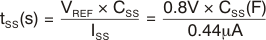 where tSS(s) = soft-start time in seconds.
where tSS(s) = soft-start time in seconds.