SLVS389M September 2002 – September 2015 TPS786
PRODUCTION DATA.
- 1 Features
- 2 Applications
- 3 Description
- 4 Revision History
- 5 Pin Configuration and Functions
- 6 Specifications
- 7 Detailed Description
- 8 Application and Implementation
- 9 Power Supply Recommendations
- 10Layout
- 11Device and Documentation Support
- 12Mechanical, Packaging, and Orderable Information
パッケージ・オプション
メカニカル・データ(パッケージ|ピン)
サーマルパッド・メカニカル・データ
発注情報
10 Layout
10.1 Layout Guidelines
To improve AC measurements like PSRR, output noise, and transient response, TI recommends designing the board with separate ground planes for VIN and VOUT, with each ground plane connected only at the ground pin of the device. In addition, the ground connection for the bypass capacitor should connect directly to the ground pin of the device.
10.2 Layout Examples
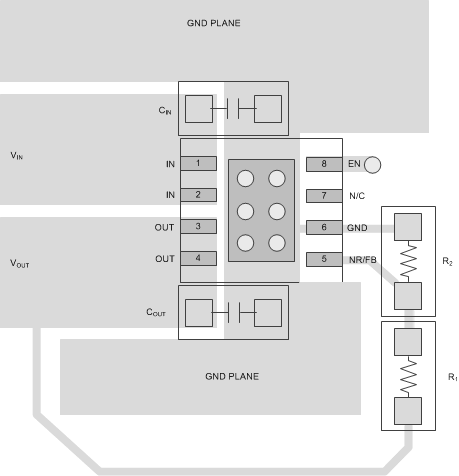 Figure 30. Recommended Layout – Adjustable-Voltage Version
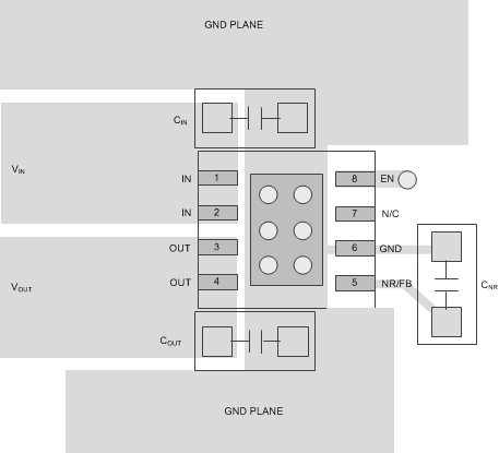 Figure 31. Recommended Layout – Fixed-Voltage Version
10.3 Regulator Mounting
The tab of the SOT223-6 package is electrically connected to ground. For best thermal performance, the tab of the surface-mount version should be soldered directly to a circuit-board copper area. Increasing the copper area improves heat dissipation.
Solder pad footprint recommendations for the devices are presented in Application Report SBFA015, Solder Pad Recommendations for Surface-Mount Devices, available from the TI website at www.ti.com.
10.4 Power Dissipation
Knowing the device power dissipation and proper sizing of the thermal plane that is connected to the tab or pad is critical to avoiding thermal shutdown and ensuring reliable operation.
Power dissipation of the device depends on input voltage and load conditions and can be calculated using Equation 4:

Power dissipation can be minimized and greater efficiency can be achieved by using the lowest possible input voltage necessary to achieve the required output voltage regulation.
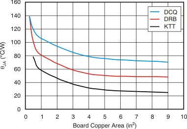
On the SON (DRB) package, the primary conduction path for heat is through the exposed pad to the printed-circuit-board (PCB). The pad can be connected to ground or be left floating; however, it should be attached to an appropriate amount of copper PCB area to ensure the device does not overheat. On both SOT-223 (DCQ) and DDPAK (KTT) packages, the primary conduction path for heat is through the tab to the PCB. That tab should be connected to ground. The maximum junction-to-ambient thermal resistance depends on the maximum ambient temperature, maximum device junction temperature, and power dissipation of the device and can be calculated using Equation 5:

Knowing the maximum RθJA, the minimum amount of PCB copper area needed for appropriate heatsinking can be estimated using Figure 32.
NOTE:
θJA value at board size of 9in2 (that is, 3in × 3in) is a JEDEC standard.Figure 32 shows the variation of θJA as a function of ground plane copper area in the board. It is intended only as a guideline to demonstrate the effects of heat spreading in the ground plane and should not be used to estimate actual thermal performance in real application environments.
NOTE
When the device is mounted on an application PCB, TI strongly recommends using ΨJT and ΨJB, as explained in the section.
10.4.1 Estimating Junction Temperature
Using the thermal metrics ΨJT and ΨJB, as shown in the Thermal Information table, the junction temperature can be estimated with corresponding formulas (given in Equation 6). For backwards compatibility, an older θJC,Top parameter is listed as well.

where
- PD is the power dissipation shown by Equation 5.
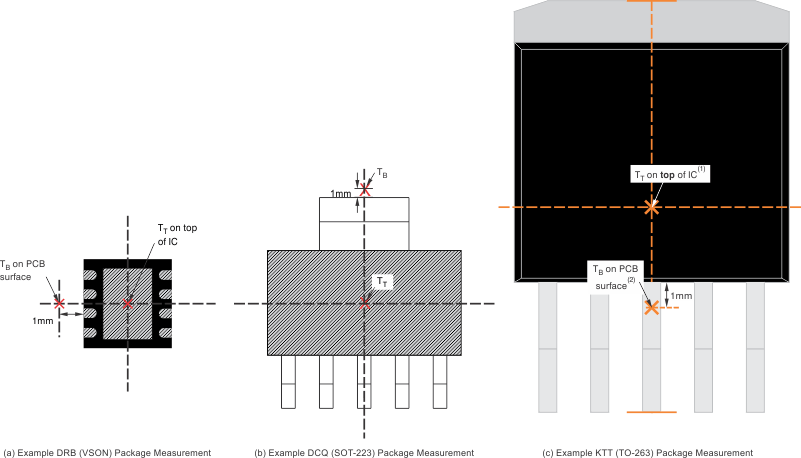
- TT is the temperature at the center-top of the IC package.
- TB is the PCB temperature measured 1mm away from the IC package on the PCB surface (as Figure 34 shows).
NOTE
Both TT and TB can be measured on actual application boards using a thermo‐gun (an infrared thermometer).
For more information about measuring TT and TB, see the application note SBVA025, Using New Thermal Metrics, available for download at www.ti.com.
By looking at Figure 33, the new thermal metrics (ΨJT and ΨJB) have very little dependency on board size. That is, using ΨJT or ΨJB with Equation 6 is a good way to estimate TJ by simply measuring TT or TB, regardless of the application board size.
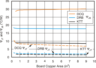 Figure 33. ΨJT and ΨJB vs Board Size
For a more detailed discussion of why TI does not recommend using θJC(top) to determine thermal characteristics, see application report Using New Thermal Metrics, SBVA025, available for download at www.ti.com. For further information, see application report IC Package Thermal Metrics, SPRA953, also available on the TI website.
