JAJSGI3B December   2011  – November 2018 TPS7A4101

PRODUCTION DATA.  

  1. 特長
  2. アプリケーション
  3. 概要
    1.     Device Images
      1.      代表的なアプリケーションの図
  4. 改訂履歴
  5. Pin Configuration and Functions
    1.     Pin Functions
  6. Specifications
    1. 6.1 Absolute Maximum Ratings
    2. 6.2 ESD Ratings
    3. 6.3 Recommended Operating Conditions
    4. 6.4 Thermal Information
    5. 6.5 Electrical Characteristics
    6. 6.6 Typical Characteristics
  7. Detailed Description
    1. 7.1 Overview
    2. 7.2 Functional Block Diagram
    3. 7.3 Feature Description
      1. 7.3.1 Enable Pin Operation
      2. 7.3.2 Thermal Protection
    4. 7.4 Device Functional Modes
      1. 7.4.1 Normal Operation
      2. 7.4.2 Dropout Operation
      3. 7.4.3 Disabled
  8. Application and Implementation
    1. 8.1 Application Information
      1. 8.1.1 Adjustable Operation
      2. 8.1.2 Transient Voltage Protection
    2. 8.2 Typical Application
      1. 8.2.1 Design Requirements
      2. 8.2.2 Detailed Design Procedure
        1. 8.2.2.1 Capacitor Recommendations
        2. 8.2.2.2 Input and Output Capacitor Requirements
        3. 8.2.2.3 Bypass Capacitor Requirements
        4. 8.2.2.4 Maximum AC Performance
        5. 8.2.2.5 Transient Response
      3. 8.2.3 Application Curve
  9. Power Supply Recommendations
  10. 10Layout
    1. 10.1 Layout Guidelines
      1. 10.1.1 Thermal Considerations
      2. 10.1.2 Power Dissipation
      3. 10.1.3 Package Mounting
    2. 10.2 Layout Example
  11. 11デバイスおよびドキュメントのサポート
    1. 11.1 ドキュメントの更新通知を受け取る方法
    2. 11.2 コミュニティ・リソース
    3. 11.3 商標
    4. 11.4 静電気放電に関する注意事項
    5. 11.5 Glossary
  12. 12メカニカル、パッケージ、および注文情報

パッケージ・オプション

メカニカル・データ(パッケージ|ピン)
サーマルパッド・メカニカル・データ
発注情報

Adjustable Operation

The TPS7A4101 has an output voltage range of approximately 1.175 V to 48 V. The nominal output voltage of the device is set by two external resistors, as shown in Figure 12.
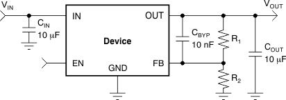
TPS7A4101 ai_adj_oper_bvs183.gifFigure 12. Adjustable Operation for Maximum AC Performance

R1 and R2 can be calculated for any output voltage range using the formula shown in Equation 1. To ensure stability under no-load conditions, this resistive network must provide a current greater than or equal to 10 µA.

Equation 1. TPS7A4101 q_r1_bvs183.gif

If greater voltage accuracy is required, take into account the output voltage offset contributions because of the feedback pin current and use 0.1% tolerance resistors.