SBVS197F May 2013 – October 2015 TPS7A8300
PRODUCTION DATA.
- 1 Features
- 2 Applications
- 3 Description
- 4 Revision History
- 5 Pin Configurations and Functions
- 6 Specifications
-
7 Detailed Description
- 7.1 Overview
- 7.2 Functional Block Diagram
- 7.3
Feature Description
- 7.3.1 ANY-OUT Programmable Output Voltage
- 7.3.2 Adjustable Operation
- 7.3.3 ANY-OUT Operation
- 7.3.4 2-A LDO with an Internal Charge Pump
- 7.3.5 Low-Noise, 0.8-V Reference
- 7.3.6 Internal Protection Circuitry
- 7.3.7 Programmable Soft-Start
- 7.3.8 Power-Good Function
- 7.3.9 Integrated Resistance Network (ANY-OUT)
- 7.4 Device Functional Modes
- 8 Application and Implementation
- 9 Power-Supply Recommendations
- 10Layout
- 11Device and Documentation Support
- 12Mechanical, Packaging, and Orderable Information
パッケージ・オプション
メカニカル・データ(パッケージ|ピン)
サーマルパッド・メカニカル・データ
発注情報
8 Application and Implementation
NOTE
Information in the following applications sections is not part of the TI component specification, and TI does not warrant its accuracy or completeness. TI’s customers are responsible for determining suitability of components for their purposes. Customers should validate and test their design implementation to confirm system functionality.
8.1 Application Information
The TPS7A8300 is a linear voltage regulator operating from 1.1 V to 6.5 V on the input and regulates voltages between 0.8 V to 5.0 V with a 1% accuracy and a 2-A maximum output current. Efficiency is defined by the ratio of output voltage to input voltage because the TPS7A8300 is a linear voltage regulator. To achieve high efficiency, the dropout voltage (VIN – VOUT) must be as small as possible, thus requiring a very low dropout LDO. Successfully implementing an LDO in an application depends on the application requirements. If the requirements are simply input voltage and output voltage, compliance specifications (such as internal power dissipation or stability) must be verified to ensure a solid design. If timing, startup, noise, PSRR, or any other transient specification is required, the design becomes more challenging. This section discusses the implementation and behavior of the TPS7A8300 LDO.
8.1.1 Start-Up
8.1.1.1 Enable (EN) and Undervoltage Lockout (UVLO)
The TPS7A8300 only turns on when both EN and UVLO are above the respective voltage thresholds. The UVLO circuit monitors input and bias voltage (VIN and VBIAS, respectively) to prevent device turn-on before VIN and VBIAS rise above the lockout voltage. The UVLO circuit also causes a shutdown when VIN and VBIAS fall below lockout. The EN signal allows independent logic-level turn-on and shutdown of the LDO. If the device turn-on is required to be controlled, the device must be enabled with or after VIN. Connect EN to VIN if turn-on control of the output voltage is not needed.
8.1.1.2 Noise-Reduction and Soft-Start Capacitor (CNR/SS)
The TPS7A8300 features a programmable, monotonic, voltage-controlled soft-start that is set with an external capacitor (CNR/SS).This soft-start eliminates power-up initialization problems when powering field-programmable gate arrays (FPGAs), digital signal processors (DSPs), or other processors. The controlled voltage ramp of the output also reduces peak inrush current during start-up, minimizing start-up transients to the input power bus.
To achieve a linear and monotonic start-up, the TPS7A8300 error amplifier tracks the voltage ramp of the external soft-start capacitor until the voltage exceeds the internal reference. The soft-start ramp time depends on the soft-start charging current (INR/SS), the soft-start capacitance (CNR/SS), and the internal reference (VREF). Soft-start ramp time can be calculated with Equation 6:
Note that INR/SS is provided in the Electrical Characteristics table and has a typical value of 6.2 µA.
For low-noise applications, the noise-reduction capacitor (connected to the NR/SS pin of the LDO) forms an RC filter for filtering out noise that is ordinarily amplified by the control loop and appears on the output voltage. For low-noise applications, a 10-nF to 1-µF CNR/SS is recommended.
8.1.1.3 Soft-Start and Inrush Current
Soft-start refers to the ramp-up characteristic of the output voltage during LDO turn-on after EN and UVLO achieve threshold voltage. The noise-reduction capacitor serves a dual purpose of both governing output noise reduction and programming the soft-start ramp during turn-on.
Inrush current is defined as the current into the LDO at the IN pin during start-up. Inrush current then consists primarily of the sum of load and current used to charge the output capacitor. This current is difficult to measure because the input capacitor must be removed, which is not recommended. However, this soft-start current can be estimated by Equation 7:

where
- VOUT(t) is the instantaneous output voltage of the turn-on ramp,
- dVOUT(t) / dt is the slope of the VOUT ramp, and
- RLOAD is the resistive load impedance.
8.1.2 Capacitor Recommendation
The TPS7A8300 is designed to be stable using low equivalent series resistance (ESR) ceramic capacitors at the input, output, and noise-reduction pin (NR, pin 13). Multilayer ceramic capacitors have become the industry standard for these types of applications and are recommended, but must be used with good judgment. Ceramic capacitors that employ X7R-, X5R-, and COG-rated dielectric materials provide relatively good capacitive stability across temperature, whereas the use of Y5V-rated capacitors is discouraged precisely because the capacitance varies so widely. In all cases, ceramic capacitance varies a great deal with operating voltage and temperature and the design engineer must be aware of these characteristics. As a rule of thumb, ceramic capacitors are recommended to be derated by 50%. To compensate for this derating, increase capacitor value by 100%. The input and output capacitors recommended herein account for a capacitance derating of 50%.
Attention must be given to the input capacitance to minimize transient input droop during load current steps. Input capacitances of 10 µF or greater provide the desired effect and do not affect stability. Note that simply using large ceramic input capacitances can also cause unwanted ringing at the output if the input capacitor (in combination with the wire-lead inductance) creates a high-Q peaking effect during transients. For example, a 5-nH lead inductance and a 10-µF input capacitor form an LC filter with a resonance frequency of 712 kHz that is near the edge of the open-loop bandwidth. Short, well-designed interconnect traces to the up-stream supply minimize this effect without adding damping. Damping of unwanted ringing can be accomplished by using a tantalum capacitor, with a few hundred milliohms of ESR, in parallel with the ceramic input capacitor.
8.1.2.1 Input and Output Capacitor Requirements (CIN and COUT)
The TPS7A8300 is designed and characterized for operation with ceramic capacitors of 22 µF or greater at the output and 10 µF at the input. Locate the input and output capacitors as near as practical to the respective input and output pins.
8.1.2.2 Feed-Forward Capacitor (CFF)
Although a feed-forward capacitor (CFF), from the FB pin to the OUT pin is not required to achieve stability, a 10-nF, feed-forward capacitor optimizes the noise and PSRR performance. A higher capacitance CFF can be used; however, the startup time is longer and the power-good signal may incorrectly indicate the output voltage has settled. For a detailed description, see application report Pros and Cons of Using a Feed-Forward Capacitor with a Low Dropout Regulator, SBVA042.
8.1.3 AC Performance
The LDO ac performance is typically understood to include power-supply rejection ratio, load step transient response, and output noise. These metrics are primarily a function of open-loop gain and bandwidth, phase margin, and reference noise.
8.1.3.1 Power-Supply Ripple Rejection (PSRR)
PSRR is a measure of how well the LDO control loop rejects ripple noise from the input source to make the dc output voltage as noise-free as possible across the frequency spectrum (usually 10 Hz to 10 MHz). Even though PSRR is therefore a loss in noise signal amplitude (the output ripple relative to the input ripple), the PSRR reciprocal is plotted in the Electrical Characteristics as a positive number in decibels (dB) for convenience. Equation 8 gives the PSRR calculation as a function of frequency where input noise voltage [VS(IN)(f)] and output noise voltage [VS(OUT)(f)] are understood to be purely ac signals.

Noise that couples from the input to the internal reference voltage for the control loop is also a primary contributor to reduced PSRR magnitude and bandwidth. This reference noise is greatly filtered by the noise-reduction capacitor at the NR pin of the LDO in combination with an internal filter resistor (RSS) for improved PSRR.
The LDO is often employed not only as a dc-dc regulator, but also to provide exceptionally clean power-supply voltages that exhibit ultra-low noise and ripple to power-sensitive system components. This usage is especially true for the TPS7A8300.
8.1.3.2 Load-Step Transient Response
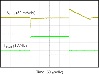
The load-step transient response is the output voltage response by the LDO to a step change in load current, whereby output voltage regulation is maintained. The worst-case response is characterized for a load step of
10 mA to 2 A (at 1 A per microsecond) and shows a classic critically-damped response of a very stable system. The voltage response shows a small dip in the output voltage when charge is initially depleted from the output capacitor and then the output recovers when the control loop adjusts itself. The depth of charge depletion immediately after the load step is directly proportional to the amount of output capacitance. However, to some extent, recovery speed is inversely proportional to that same output capacitance. In other words, larger output capacitances act to decrease any voltage dip or peak occurring during a load step but also decrease the control-loop bandwidth, thereby slowing response.
The worst-case off-loading step characterization occurs when the current step transitions from 2 A to 0 mA. Initially, the LDO loop cannot respond fast enough to prevent a small increase in output voltage charge on the output capacitor. The LDO cannot sink charge, therefore the control loop must turn off the main pass-FET to wait for the charge to deplete.
8.1.3.3 Noise
The TPS7A8300 is designed for system applications where minimizing noise on the power-supply rail is critical to system performance. This scenario is the case for phase-locked loop (PLL)-based clocking circuits where minimum phase noise is all important, or in test and measurement systems where even small power-supply noise fluctuations can distort instantaneous measurement accuracy.
LDO noise is defined as the internally-generated intrinsic noise created by the semiconductor circuits alone. This noise is the sum of various types of noise (such as shot noise associated with current-through-pin junctions, thermal noise caused by thermal agitation of charge carriers, flicker noise, or 1/f noise that is a property of resistors and dominates at lower frequencies as a function of 1/f, burst noise, and avalanche noise).
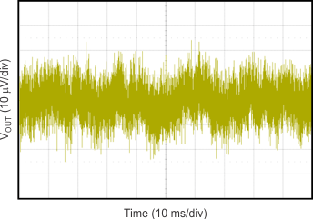
To calculate the LDO RMS output noise, a spectrum analyzer must first measure the spectral noise across the bandwidth of choice (typically 10 Hz to 100 kHz in units of µV/√Hz). RMS noise is then calculated as the integrated square root of the squared spectral noise over the band, then averaged by the bandwidth.
8.1.3.4 Behavior when Transitioning from Steady Dropout into Regulation
When the device is in a steady dropout state (defined as when the device is in dropout, VIN < VOUT(NOM) + VDO, right after being in a normal regulation state, but not during startup), the pass-FET is driven as hard as possible when the control loop is out of balance. During the normal time required for the device to regain regulation, VIN ≥ VOUT(NOM) + VDO, VOUT overshoots if the input voltage slew rate is 0.1 V/µs or faster.
8.1.4 Power Dissipation (PD)
Circuit reliability demands that proper consideration be given to device power dissipation, location of the circuit on the printed circuit board (PCB), and correct sizing of the thermal plane. The PCB area around the regulator must be as free as possible of other heat-generating devices that cause added thermal stresses.
To first-order approximation, power dissipation in the regulator depends on the input-to-output voltage difference and load conditions. PD can be calculated using Equation 9:

An important note is that power dissipation can be minimized, and thus greater efficiency achieved, by proper selection of the system voltage rails. Proper selection allows the minimum input voltage necessary for output regulation to be obtained.
The primary heat conduction path for the VQFN (RGW and RGR) package is through the thermal pad to the PCB. Solder the thermal pad to a copper pad area under the device. This pad area contains an array of plated vias that conduct heat to any inner plane areas or to a bottom-side copper plane.
The maximum power dissipation determines the maximum allowable junction temperature (TJ) for the device. Power dissipation and junction temperature are most often related by the junction-to-ambient thermal resistance (θJA) of the combined PCB and device package and the temperature of the ambient air (TA), according to Equation 10.

Unfortunately, this thermal resistance (θJA) is highly dependent on the heat-spreading capability built into the particular PCB design, and therefore varies according to the total copper area, copper weight, and location of the planes. The θJA recorded in the Thermal Information table is determined by the JEDEC standard, PCB, and copper-spreading area and is only used as a relative measure of package thermal performance. Note that for a well-designed thermal layout, θJA is actually the sum of the VQFN package junction-to-case (bottom) thermal resistance (θJCbot) plus the thermal resistance contribution by the PCB copper. When θJCbot is known, the amount of heat-sinking area required can be estimated for a given θJA, as shown in Figure 53. θJCbot can be found in the Thermal Information table.

8.1.5 Estimating Junction Temperature
The JEDEC standard now recommends the use of psi (Ψ) thermal metrics to estimate the junction temperatures of the LDO when in-circuit on a typical PCB board application. These metrics are not strictly speaking thermal resistances, but rather offer practical and relative means of estimating junction temperatures. These psi metrics are determined to be significantly independent of the copper-spreading area. The key thermal metrics (ΨJT and ΨJB) are given in the Thermal Information table and are used in accordance with Equation 11.

where
- PD is the power dissipated as explained in Equation 9,
- TT is the temperature at the center-top of the device package, and
- TB is the PCB surface temperature measured 1 mm from the device package and centered on the package edge.
8.2 Typical Application
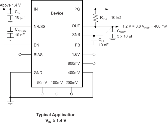
This section discusses the implementation of the TPS7A8300 using the ANY-OUT configuration to regulate a 1.6-A load requiring good PSRR at high frequency with low-noise at 1.2 V using a 1.4-V input voltage. The schematic for this typical application circuit is provided in Figure 54.
 Figure 54. Typical Application
8.2.1 Design Requirements
For this design example, use the parameters listed in Table 4 as the input parameters.
Table 4. Design Parameters
| PARAMETER | DESIGN REQUIREMENT |
|---|---|
| Input voltage | 1.4 V, ±3%, provided by the dc/dc converter switching at 1 MHz |
| Output voltage | 1.2 V, ±1% |
| Output current | 1.6 A (maximum), 10 mA (minimum) |
| RMS noise, 10 Hz to 100 kHz | < 20 µVRMS |
| PSRR at 1 MHz | > 40 dB |
| Startup time | < 10 ms |
8.2.2 Detailed Design Procedure
At 1.6 A, the dropout of the TPS7A8300 has 150 mV maximum dropout over temperature, thus a 200-mV headroom is sufficient for operation over both input and output voltage accuracy. The efficiency of the TPS7A8300 in this configuration is VOUT / VIN = 85.7%.
To achieve the smallest form factor, the 3.5-mm × 3.5-mm2 RGR package is selected. The ANY-OUT internal resistor network is also used.
To achieve 1.2 V on the output, the 400mV pin is grounded. The voltage value of 400 mV is added to the 0.8-V internal reference voltage for VOUT(NOM) equal to 1.2 V; as described in Equation 12.
Input and output capacitors are selected in accordance with the Capacitor Recommendation section. Ceramic capacitances of 10 µF for the input and three 10-µF capacitors for the output are selected.
To satisfy the required startup time and still maintain low noise performance, a 10-nF CNR/SS is selected. This value is calculated with Equation 13.
With an efficiency of 85.7% and a 1.6-A maximum load, the internal power dissipation is 320 mW, which corresponds to a 11.3°C junction temperature rise for the RGR package. With an 85°C maximum ambient temperature, the junction temperature is at 96.3°C. To minimize noise, a feed-forward capacitance (CFF) of 10 nF is selected.
8.2.3 Application Curves
 Figure 55. Output Load Transient Response
 Figure 56. 10-Hz to 100-kHz Output Noise Voltage, 1.6-A Load Current
8.3 Do's and Don'ts
Do place at least one 22-µF ceramic capacitor as close as possible to the OUT terminal of the regulator.
Do not place the output capacitor more than 10 mm away from the regulator.
Do connect a 10-μF low equivalent series resistance (ESR) capacitor across the IN pin and GND input of the regulator.
Do not exceed the absolute maximum ratings.
Do not float the Enable pin.