SBVS313 June 2017 TPS7A85A
PRODUCTION DATA.
- 1 Features
- 2 Applications
- 3 Description
- 4 Revision History
- 5 Pin Configuration and Functions
- 6 Specifications
- 7 Detailed Description
-
8 Application and Implementation
- 8.1
Application Information
- 8.1.1
External Component Selection
- 8.1.1.1 Adjustable Operation
- 8.1.1.2 ANY-OUT Programmable Output Voltage
- 8.1.1.3 ANY-OUT Operation
- 8.1.1.4 Increasing ANY-OUT Resolution for LILO Conditions
- 8.1.1.5 Current Sharing
- 8.1.1.6 Recommended Capacitor Types
- 8.1.1.7 Input and Output Capacitor Requirements (CIN and COUT)
- 8.1.1.8 Feed-Forward Capacitor (CFF)
- 8.1.1.9 Noise-Reduction and Soft-Start Capacitor (CNR/SS)
- 8.1.2 Start-Up
- 8.1.3 AC and Transient Performance
- 8.1.4 DC Performance
- 8.1.5 Sequencing Requirements
- 8.1.6 Negatively Biased Output
- 8.1.7 Reverse Current
- 8.1.8 Power Dissipation (PD)
- 8.1.1
External Component Selection
- 8.2 Typical Applications
- 8.1
Application Information
- 9 Power-Supply Recommendations
- 10Layout
パッケージ・オプション
メカニカル・データ(パッケージ|ピン)
- RGR|20
サーマルパッド・メカニカル・データ
- RGR|20
発注情報
1 Features
- Low Dropout: 150 mV (Typical) at 4 A
- 0.75% (Maximum) Accuracy Over Line, Load, and Temperature With BIAS
- Output Voltage Noise:
- 4.4 μVRMS at 0.8-V Output
- 7.7 μVRMS at 5.1-V Output
- Input Voltage Range:
- Without BIAS: 1.4 V to 6.5 V
- With BIAS: 1.1 V to 6.5 V
- ANY-OUT™ Operation:
- Output Voltage Range: 0.8 V to 3.95 V
- Adjustable Operation:
- Output Voltage Range: 0.8 V to 5.1 V
- Power-Supply Ripple Rejection:
- 40 dB at 500 kHz
- Excellent Load Transient Response
- Adjustable Soft-Start In-Rush Control
- Open-Drain Power-Good (PG) Output
- Stable with a 47-μF or Larger Ceramic Output Capacitor
- θJC = 3.4°C/W
- 3.5-mm × 3.5-mm, 20-Pin VQFN
2 Applications
- Digital Loads: SerDes, FPGAs, and DSPs
- Instrumentation, Medical, and Audio
- High-Speed Analog Circuits:
- VCO, ADC, DAC, and LVDS
- Imaging: CMOS Sensors and Video ASICs
- Test and Measurement
3 Description
The TPS7A85A is a low-noise (4.4 μVRMS), low dropout linear regulator (LDO) capable of sourcing 4 A with only 240 mV of maximum dropout. The device output voltage is pin-programmable from 0.8 V to 3.95 V and adjustable from 0.8 V to 5.1 V using an external resistor divider.
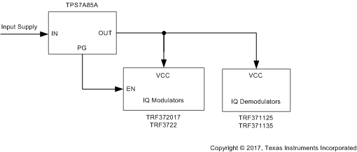
The combination of low-noise (4.4 μVRMS), high- PSRR, and high output current capability makes the TPS7A85A ideal to power noise-sensitive components such as those found in high-speed communications, video, medical, or test and measurement applications. The high performance of the TPS7A85A limits power-supply-generated phase noise and clock jitter, making this device ideal for powering high-performance serializer and deserializer (SerDes), analog-to-digital converters (ADCs), digital-to-analog converters (DACs), and RF components. Specifically, RF amplifiers benefit from the high-performance and 5.1-V output capability of the device.
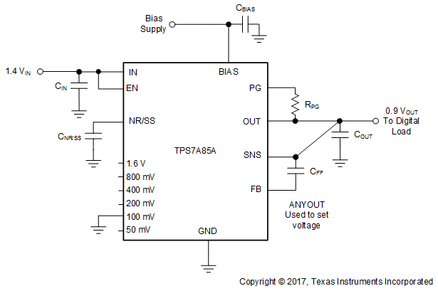
For digital loads (such as application-specific integrated circuits (ASICs), field-programmable gate arrays (FPGAs), and digital signal processors (DSPs)) requiring low-input voltage, low-output (LILO) voltage operation, the exceptional accuracy (0.75% over load and temperature), remote sensing, excellent transient performance, and soft-start capabilities of the TPS7A85A ensure optimal system performance.
The versatility of the TPS7A8500A makes the device a component of choice for many demanding applications.
Device Information(1)
| PART NUMBER | PACKAGE | BODY SIZE (NOM) |
|---|---|---|
| TPS7A85A | VQFN (20) | 3.50 mm × 3.50 mm |
- For all available packages, see the orderable addendum at the end of the data sheet.
Powering RF Components

Powering Digital Loads
