JAJSC97C January 2015 – September 2018 TPS7B7701-Q1 , TPS7B7702-Q1
PRODUCTION DATA.
- 1 特長
- 2 アプリケーション
- 3 概要
- 4 改訂履歴
- 5 Pin Configuration and Functions
- 6 Specifications
-
7 Detailed Description
- 7.1 Overview
- 7.2 Functional Block Diagram
- 7.3
Feature Description
- 7.3.1 Fault Detection and Protection
- 7.3.2 Short-Circuit and Overcurrent Protection
- 7.3.3 Short-to-Battery and Reverse Current Detection
- 7.3.4 Thermal Shutdown
- 7.3.5 Integrated Reverse-Polarity Protection
- 7.3.6 Integrated Inductive Clamp
- 7.3.7 Undervoltage Lockout
- 7.3.8 Enable (EN, EN1, and EN2)
- 7.3.9 Internal Voltage Regulator (VCC)
- 7.3.10 Current Sense Multiplexing
- 7.3.11 Adjustable Output Voltage (FB, FB1, and FB2)
- 7.4 Device Functional Modes
- 8 Application and Implementation
- 9 Power Supply Recommendations
- 10Layout
- 11デバイスおよびドキュメントのサポート
- 12メカニカル、パッケージ、および注文情報
パッケージ・オプション
メカニカル・データ(パッケージ|ピン)
- PWP|16
サーマルパッド・メカニカル・データ
- PWP|16
発注情報
7.3.1 Fault Detection and Protection
The device includes both analog current sense and digital fault pins for full diagnostics of different fault conditions.
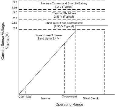
The current-sense voltage scale is selected based on the output-current range of interest. Figure 19 shows a recommended setting that allows for full diagnostics of each fault. Before the device goes into current-limit mode, the output current-sense voltage is linearly proportional to the actual load current. During a thermal-shutdown (TSD) and short-to-battery (STB) condition, the current-sense voltage is set to the fault voltage level that is specified in the Electrical Characteristics table.
 Figure 19. Functionality of the Current-Sense Output