JAJSPU0B February 2023 – December 2023 TPS7H3302-SEP , TPS7H3302-SP
PRODUCTION DATA
- 1
- 1 特長
- 2 アプリケーション
- 3 概要
- 4 Device Options
- 5 Pin Configuration and Functions
- 6 Specifications
- 7 Detailed Description
-
8 Application and Implementation
- 8.1 Application Information
- 8.2
Typical Application
- 8.2.1 Design Requirements
- 8.2.2
Detailed Design Procedure
- 8.2.2.1 VDD Capacitor
- 8.2.2.2 VLDO Input Capacitor
- 8.2.2.3 VTT Output Capacitor
- 8.2.2.4 VTTSNS Connection
- 8.2.2.5 Low VDD Applications
- 8.2.2.6 S3 and Pseudo-S5 Support
- 8.2.2.7 Tracking Startup and Shutdown
- 8.2.2.8 Output Tolerance Consideration for VTT DIMM or Module Applications
- 8.2.2.9 LDO Design Guidelines
- 8.2.3 Application Curve
- 8.3 Power Supply Recommendations
- 8.4 Layout
- 9 Device and Documentation Support
- 10Revision History
- 11Mechanical, Packaging, and Orderable Information
パッケージ・オプション
デバイスごとのパッケージ図は、PDF版データシートをご参照ください。
メカニカル・データ(パッケージ|ピン)
- DAP|32
サーマルパッド・メカニカル・データ
- DAP|32
発注情報
8.2.2.9 LDO Design Guidelines
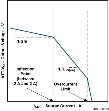
For TPS7H3302, a minimum of 420 mV (VLDOINMIN – VTTMAX) is needed in order to support a Gm driven sourcing current of 2 A based on the specified dropout voltage maximum at VDDQSNS = 1.5 V. Because the TPS7H3302 is essentially a Gm-driven LDO, its impedance characteristics are both a function of the 1/Gm and RDS(on) of the sourcing MOSFET (see TPS7H3302 Impedance Characteristics). The current inflection point of the design is between 3 A and 4 A. When ISRC is less than the inflection point, the LDO is considered to be operating in the Gm region; when ISRC is greater than the inflection point but less than the overcurrent limit point, the LDO is operating in the RDS(on) region. The typical sourcing RDS(on) is 154 mΩ with VIN = 3 V and TJ = 125°C.
 Figure 8-9 TPS7H3302 Impedance
Characterisitcs