JAJSIY2D april 2019 – may 2023 TPS7H4001-SP
PRODMIX
- 1
- 1 特長
- 2 アプリケーション
- 3 概要
- 4 Revision History
- 5 Device Options Table
- 6 Pin Configuration and Functions
-
7 Specifications
- 7.1 Absolute Maximum Ratings
- 7.2 ESD Ratings
- 7.3 Recommended Operating Conditions
- 7.4 Thermal Information
- 7.5 Electrical Characteristics - All Devices
- 7.6 Electrical Characteristics: CDFP and KGD Options
- 7.7 Electrical Characteristics: HTSSOP (SHP) Option
- 7.8 Electrical Characteristics: HTSSOP (QMLP) Option
- 7.9 Quality Conformance Inspection
- 7.10 Typical Characteristics
-
8 Detailed Description
- 8.1 Overview
- 8.2 Functional Block Diagram
- 8.3
Feature Description
- 8.3.1 VIN and Power VIN Pins (VIN and PVIN)
- 8.3.2 Voltage Reference
- 8.3.3 Adjusting the Output Voltage
- 8.3.4 Safe Start-Up Into Prebiased Outputs
- 8.3.5 Error Amplifier
- 8.3.6 Enable and Adjust UVLO
- 8.3.7 Adjustable Switching Frequency and Synchronization (SYNC)
- 8.3.8 Soft-Start (SS/TR)
- 8.3.9 Power Good (PWRGD)
- 8.3.10 Sequencing
- 8.3.11 Output Overvoltage Protection (OVP)
- 8.3.12 Overcurrent Protection
- 8.3.13 Thermal Shutdown
- 8.3.14 Turn-On Behavior
- 8.3.15 Slope Compensation
- 8.3.16 Small Signal Model for Frequency Compensation
- 8.4 Device Functional Modes
-
9 Application and Implementation
- 9.1 Application Information
- 9.2
Typical Application
- 9.2.1 Design Requirements
- 9.2.2
Detailed Design Procedure
- 9.2.2.1 Operating Frequency
- 9.2.2.2 Output Inductor Selection
- 9.2.2.3 Output Capacitor Selection
- 9.2.2.4 Input Capacitor Selection
- 9.2.2.5 Soft-Start Capacitor Selection
- 9.2.2.6 Undervoltage Lockout (UVLO) Set Point
- 9.2.2.7 Output Voltage Feedback Resistor Selection
- 9.2.2.8 Compensation Component Selection
- 9.2.3 Parallel Operation
- 9.2.4 Application Curve
- 9.3 Power Supply Recommendations
- 9.4 Layout
- 10Device and Documentation Support
- 11Mechanical, Packaging, and Orderable Information
パッケージ・オプション
デバイスごとのパッケージ図は、PDF版データシートをご参照ください。
メカニカル・データ(パッケージ|ピン)
- DDW|44
- KGD|0
- HKY|34
サーマルパッド・メカニカル・データ
- DDW|44
発注情報
8.3.10 Sequencing
Many of the common power-supply sequencing methods can be implemented using the SS/TR, EN, and PWRGD pins.
The sequential method is shown in Figure 8-7 using two TPS7H4001-SP devices. The PWRGD pin of the first device is coupled to the EN pin of the second device, which enables the second power supply after the primary supply reaches regulation.
 Figure 8-7 Sequential
Start-Up Sequence
Figure 8-7 Sequential
Start-Up SequenceFigure 8-8 shows the method implementing ratiometric sequencing by connecting the SS/TR pins of two devices together. The regulator outputs ramp up and reach regulation at the same time. When calculating the soft-start time, the pullup current source must be doubled in Equation 5 as there is only one SS/TR capacitor. A similar situation applies if a resistor divider is used in the EN pin, that is, only one resistor divider is needed and the factor of 2 must be taken into account when calculating the resistor values. This ratiometric connection is the one used in primary mode as described in the Adjustable Switching Frequency and Synchronization (SYNC) section.
 Figure 8-8 Ratiometric
Start-Up Sequence
Figure 8-8 Ratiometric
Start-Up SequenceRatiometric and simultaneous power-supply sequencing can be implemented by connecting the resistor network of R1 and R2 (shown in Figure 8-9) to the output of the power supply that needs to be tracked or another voltage reference source. Using Equation 6 and Equation 7, the tracking resistors can be calculated to initiate the VOUT2 slightly before, after, or at the same time as VOUT1. Equation 8 is the voltage difference between VOUT1 and VOUT2.
To design a ratiometric start-up in which the VOUT2 voltage is slightly greater than the VOUT1 voltage when VOUT2 reaches regulation, use a negative number in Equation 6 and Equation 7 for ΔV. Equation 8 results in a positive number for applications where the VOUT2 is slightly lower than VOUT1 when VOUT2 regulation is achieved.
The ΔV variable is 0 V for simultaneous sequencing. To minimize the effect of the inherent SS/TR to VSENSE offset (VSS-OFFSET = 30 mV) in the soft-start circuit and the offset created by the pullup current source (ISS = 2.5 μA) and tracking resistors, the VSS-OFFSET and ISS are included as variables in the equations.
To ensure proper operation of the device, the calculated R1 value from Equation 6 must be greater than the value calculated in Equation 9.
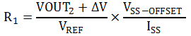
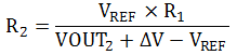
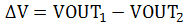

 Figure 8-9 Ratiometric and
Simultaneous Start-Up Sequence
Figure 8-9 Ratiometric and
Simultaneous Start-Up Sequence