SLVSCD1C December 2013 – November 2015 TPS92561
PRODUCTION DATA.
- 1 Features
- 2 Applications
- 3 Description
- 4 Revision History
- 5 Pin Configuration and Functions
- 6 Specifications
- 7 Detailed Description
-
8 Application and Implementation
- 8.1 Application Information
- 8.2
Typical Applications
- 8.2.1 Offline Boost Schematic for Design Example
- 8.2.2 11-W, 120-VAC Input, 225-V Output, Offline Boost Design Example
- 9 Power Supply Recommendations
- 10Layout
- 11Device and Documentation Support
- 12Mechanical, Packaging, and Orderable Information
パッケージ・オプション
メカニカル・データ(パッケージ|ピン)
- DGN|8
サーマルパッド・メカニカル・データ
- DGN|8
発注情報
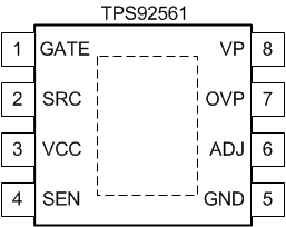
5 Pin Configuration and Functions
DGN Package
8-Pin HVSSOP
Top View

Pin Functions
| PIN | I/O | DESCRIPTION | |
|---|---|---|---|
| NAME | NO. | ||
| GATE | 1 | O | Gate driver output pin. Connect to the gate terminal of the low-side N-channel power FET. For off-line applications, use a gate resistance of ≥ 75 Ω. |
| SRC | 2 | I | Gate driver return. Connect to the source terminal of the low-side, N-channel power FET. By connecting SRC to the FET source, switching current spikes are not passed through the sense resistor. |
| VCC | 3 | O | Gate driver power rail. Connect a 0.47-µF minimum decoupling capacitor from this pin to SRC pin. |
| SEN | 4 | I | LED current sense pin. Current sense input. For off-line applications, connect to SEN and the current sensing resistor through an R-C filter with a time constant similar to the converter switching frequency. |
| GND | 5 | — | Ground. Connect to the system ground plane. |
| ADJ | 6 | I | LED current adjust pin. Converter reference. Can be connected to the converter rectified AC for high power factor, or to the LED output voltage for improved line regulation. |
| OVP | 7 | I | Overvoltage. Connect to resistor divider from VOUT (LED+) to detect overvoltage. |
| VP | 8 | I | Power supply of the integrated circuit (IC). Connect to an appropriate voltage source to provide power for the IC. (VP ≤ 42 V) See Example Circuits for example diagrams. |
| PowerPAD | — | — | Solder to printed circuit board (PCB) with or without thermal vias to enhance thermal performance. Although it can be left floating, TI recommends to connect the PowerPAD™ to GND. |