JAJSIW2 April   2020 TPS92612

PRODUCTION DATA.  

  1. 特長
  2. アプリケーション
  3. 概要
    1.     代表的なアプリケーションの図
  4. 改訂履歴
  5. Pin Configuration and Functions
    1.     Pin Functions
  6. Specifications
    1. 6.1 Absolute Maximum Ratings
    2. 6.2 ESD Ratings
    3. 6.3 Recommended Operating Conditions
    4. 6.4 Thermal Information
    5. 6.5 Electrical Characteristics
    6. 6.6 Timing Requirements
    7. 6.7 Typical Characteristics
  7. Detailed Description
    1. 7.1 Overview
    2. 7.2 Functional Block Diagram
    3. 7.3 Feature Description
      1. 7.3.1 Device Bias
        1. 7.3.1.1 Power-On Reset (POR)
      2. 7.3.2 Constant-Current Driver
      3. 7.3.3 PWM Control
      4. 7.3.4 Protection
        1. 7.3.4.1 Short-to-GND Protection
        2. 7.3.4.2 Over Temperature Protection
    4. 7.4 Device Functional Modes
      1. 7.4.1 Undervoltage Lockout, V(SUPPLY)< V(POR_rising)
      2. 7.4.2 Normal State, V(SUPPLY) ≥ 4.5 V
  8. Application and Implementation
    1. 8.1 Application Information
    2. 8.2 Typical Application
      1. 8.2.1 Single LED Driver
        1. 8.2.1.1 Design Requirements
        2. 8.2.1.2 Detailed Design Procedure
        3. 8.2.1.3 Application Curve
      2. 8.2.2 Single-Channel LED Driver With Heat Sharing
        1. 8.2.2.1 Design Requirements
        2. 8.2.2.2 Detailed Design Procedure
        3. 8.2.2.3 Application Curve
  9. Power Supply Recommendations
  10. 10Layout
    1. 10.1 Layout Guidelines
    2. 10.2 Layout Example
  11. 11デバイスおよびドキュメントのサポート
    1. 11.1 ドキュメントの更新通知を受け取る方法
    2. 11.2 サポート・リソース
    3. 11.3 商標
    4. 11.4 静電気放電に関する注意事項
    5. 11.5 Glossary
  12. 12メカニカル、パッケージ、および注文情報

パッケージ・オプション

メカニカル・データ(パッケージ|ピン)
サーマルパッド・メカニカル・データ
発注情報

Typical Characteristics

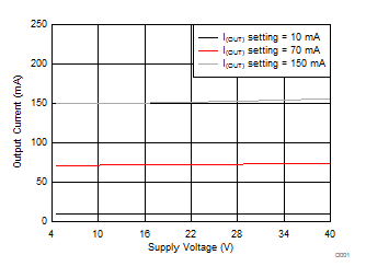
TPS92612 D001-IOUT-SUPPLY-SLDS233.gif
TA = 25 °C
Figure 2. Output Current vs Supply Voltage
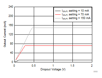
TPS92612 D002-IOUT-VDROP-SLDS233.gif
TA = 25 °C
Figure 4. Output Current vs Dropout Voltage
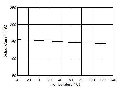
TPS92612 D005_SLVSFG3.gif
I(OUT) setting = 150 mA V(SUPPLY)-V(OUT) = 2 V
Figure 6. Output Current vs Temperature
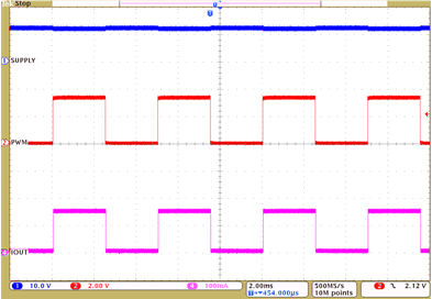
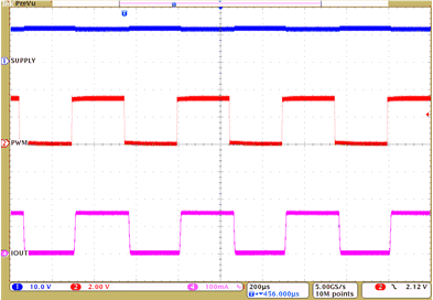
TPS92612 tps92612-typical-char-pwm-200Hz.gif
Ch. 1 = SUPPLY Ch. 2 = V(PWM) Ch. 4 = I(OUT)
f(PWM) = 200 Hz Duty-cycle = 50%
Figure 8. PWM Dimming at 200 Hz
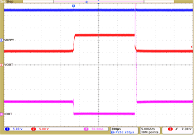
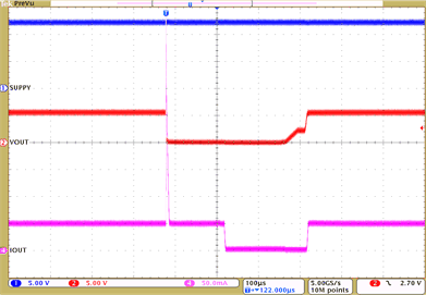
TPS92612 typ-app-led-open-circuit-slds237.gif
Ch. 1 = SUPPLY Ch. 2 = V(OUT) Ch. 4 = I(OUT)
Figure 10. LED Open-Circuit and Recovery
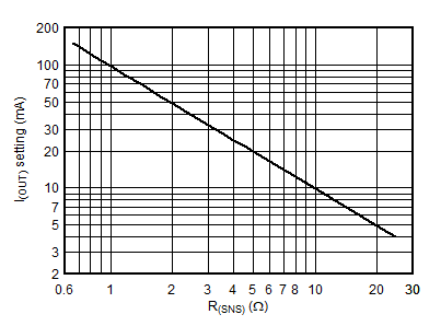
TPS92612 D002_SLVSFG3.gif
Figure 3. Output Current vs Current-Sense Resistor
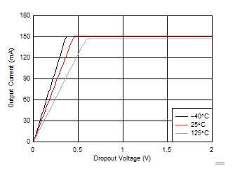
TPS92612 D003-VDROP-TEMP-SLDS233.gif
I(OUT) setting = 150 mA
Figure 5. Output Current vs Dropout Voltage
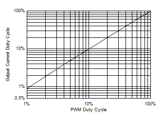
TPS92612 D005-PWMIN-OUT-SLDS233.gif
f(PWM) = 200 Hz
Figure 7. PWM Output Duty Cycle vs Input Duty Cycle
TPS92612 tps92612-typical-char-pwm-2kHz.gif
Ch. 1 = SUPPLY Ch. 2 = V(PWM) Ch. 4 = I(OUT)
f(PWM) = 2 kHz Duty-cycle = 50%
Figure 9. PWM Dimming at 2 kHz
TPS92612 typ-app-led-short-slds237.gif
Ch. 1 = SUPPLY Ch. 2 = V(OUT) Ch. 4 = I(OUT)
Figure 11. LED Short-Circuit Protection and Recovery