JAJSL38 December 2023 TPSI3100-Q1
ADVANCE INFORMATION
- 1
- 1 特長
- 2 アプリケーション
- 3 概要
- 4 Device Comparison Table
- 5 Pin Configuration and Functions
-
6 Specifications
- 6.1 Absolute Maximum Ratings
- 6.2 ESD Ratings
- 6.3 Recommended Operating Conditions
- 6.4 Thermal Information
- 6.5 Power Ratings
- 6.6 Insulation Specifications
- 6.7 Safety-Related Certifications
- 6.8 Safety Limiting Values
- 6.9 Electrical Characteristics
- 6.10 Switching Characteristics
- 6.11 Insulation Characteristic Curves
- 6.12 Typical Characteristics
- 7 Parameter Measurement Information
- 8 Detailed Description
- 9 Application and Implementation
- 10Device and Documentation Support
- 11Revision History
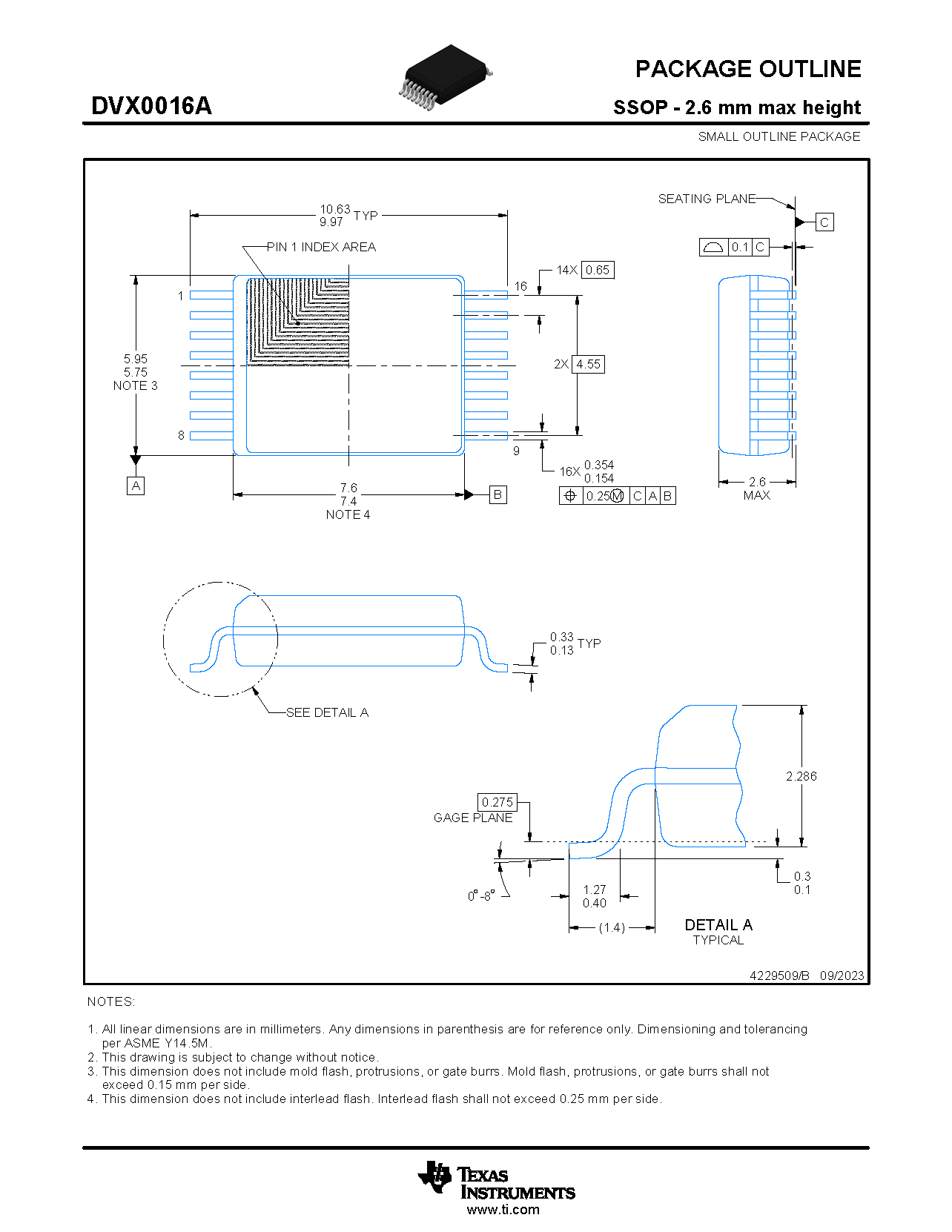
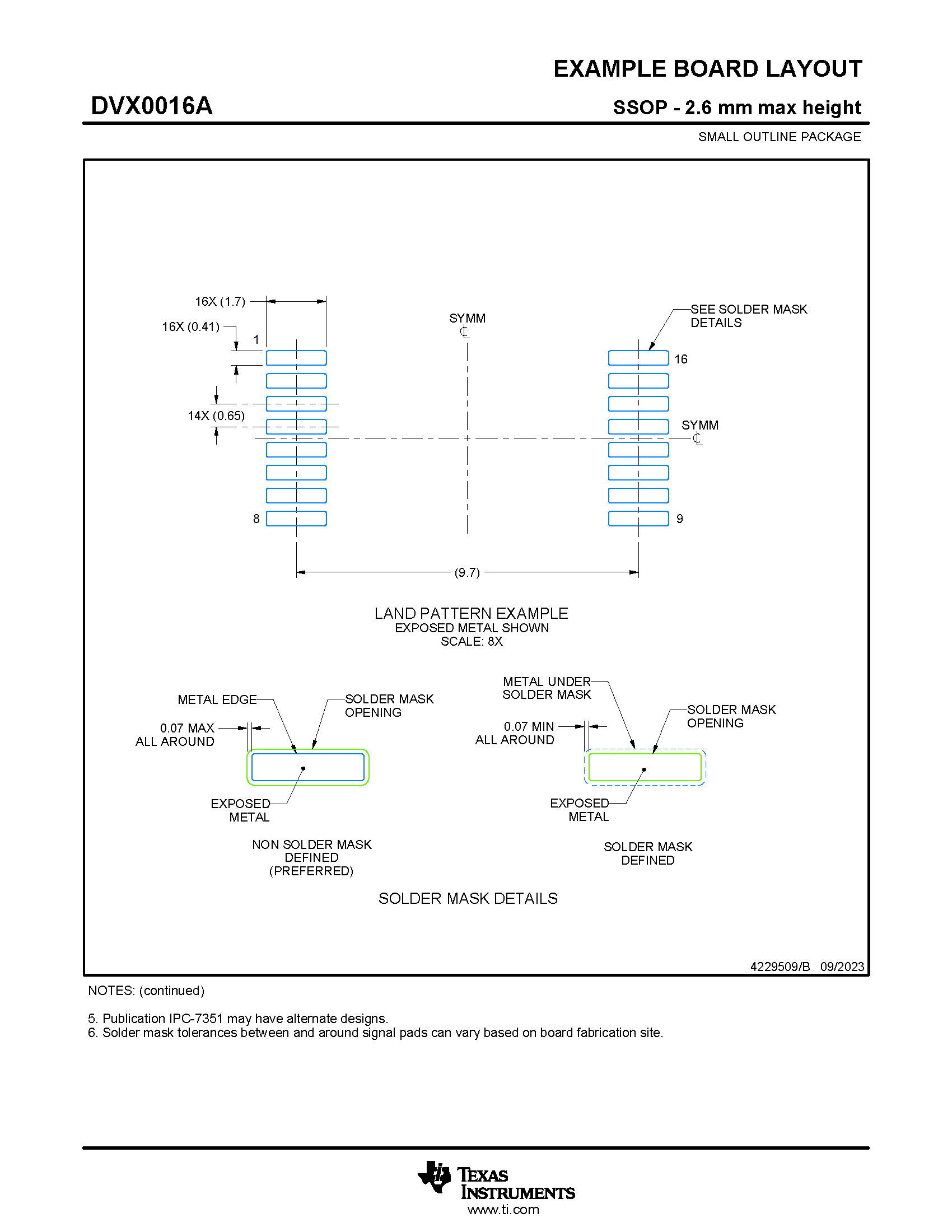
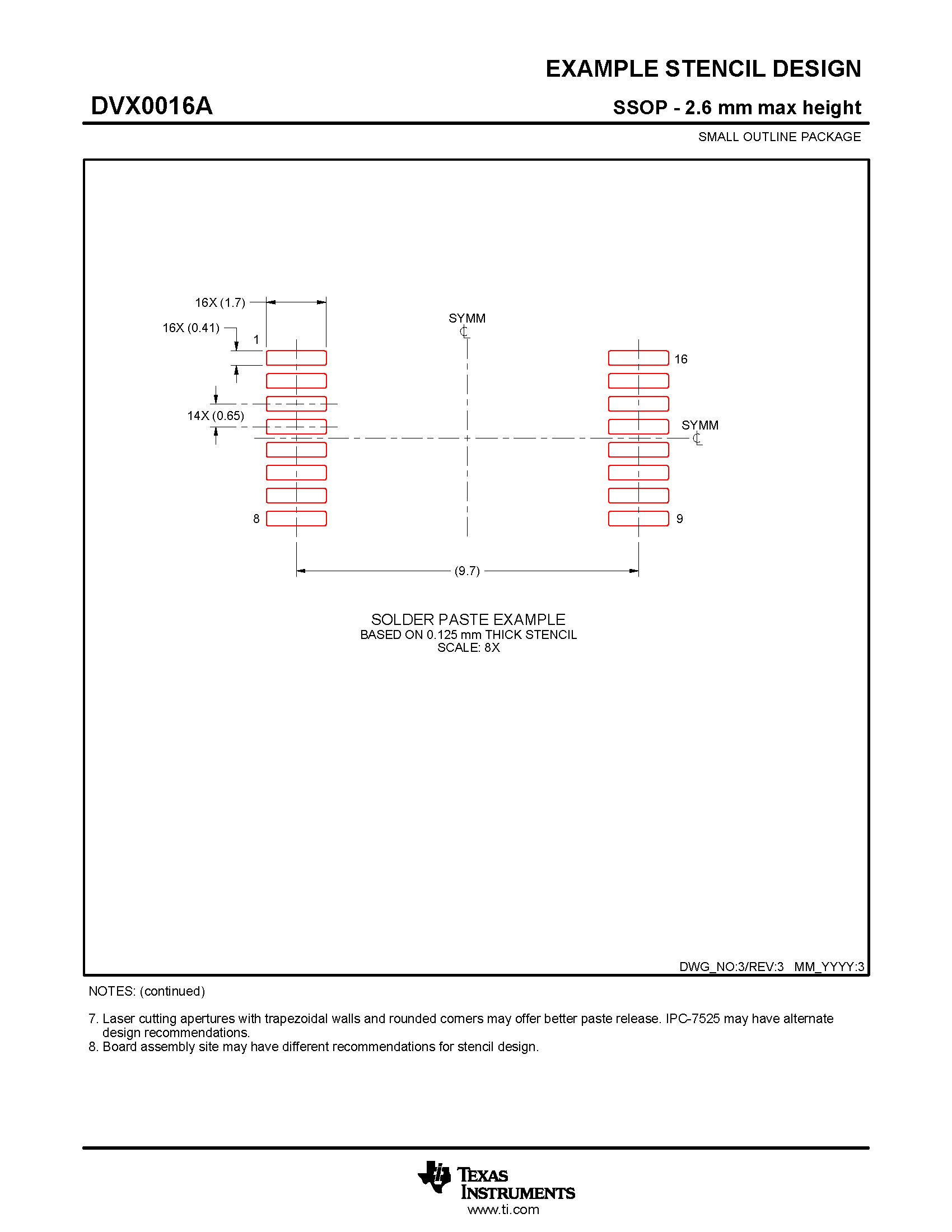
- 12Mechanical, Packaging, and Orderable Information
12.1 Tape and Reel Information
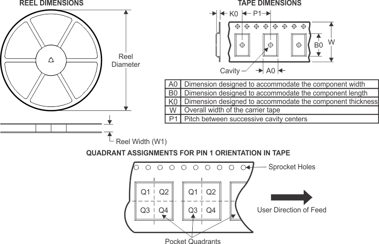
| Device | Package Type | Package Drawing | Pins | SPQ | Reel Diameter (mm) | Reel Width W1 (mm) | A0 (mm) | B0 (mm) | K0 (mm) | P1 (mm) | W (mm) | Pin1 Quadrant |
|---|---|---|---|---|---|---|---|---|---|---|---|---|
| PTPSI3100QDVXRQ1 | SSOP | DVX | 16 | 1000 | 330.0 | 16.4 | 12.05 | 6.15 | 3.3 | 16.0 | 16.0 | Q1 |
| PTPSI3100LQDVXRQ1 | SSOP | DVX | 16 | 1000 | 330.0 | 16.4 | 12.05 | 6.15 | 3.3 | 16.0 | 16.0 | Q1 |
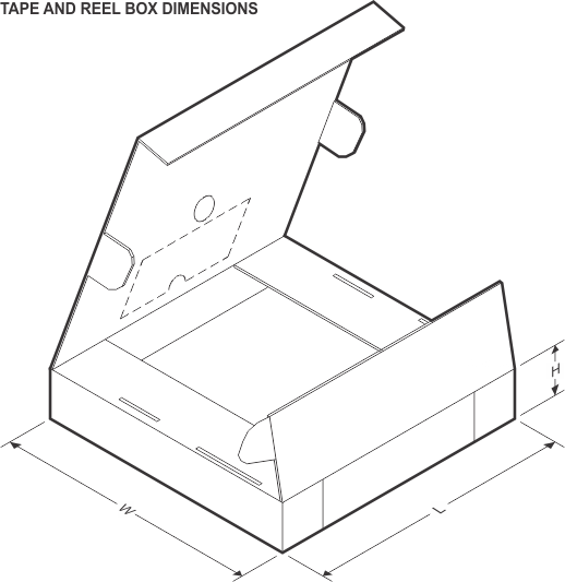
| Device | Package Type | Package Drawing | Pins | SPQ | Length (mm) | Width (mm) | Height (mm) |
|---|---|---|---|---|---|---|---|
| PTPSI3100QDVXRQ1 | SSOP | DVX | 16 | 1000 | 350.0 | 350.0 | 43.0 |
| PTPSI3100LQDVXRQ1 | SSOP | DVX | 16 | 1000 | 350.0 | 350.0 | 43.0 |