JAJSI06A September 2019 – December 2020 TPSM82810 , TPSM82813
PRODUCTION DATA
- 1 特長
- 2 アプリケーション
- 3 概要
- 4 Revision History
- 5 Device Comparison Table
- 6 Pin Configuration and Functions
- 7 Specifications
- 8 Parameter Measurement Information
- 9 Detailed Description
- 10Application and Implementation
- 11Power Supply Recommendations
- 12Layout
- 13Device and Documentation Support
- 14Mechanical, Packaging, and Orderable Information
9.4.4 Current Limit and Short Circuit Protection
The TPSM8281x is protected against overload and short circuit events. If the inductor current exceeds the current limit ILIMH, the high-side MOSFET is turned off and the low-side MOSFET is turned on to ramp down the inductor current. The high-side MOSFET turns on again only if the current in the low-side MOSFET has decreased below the low-side current limit. Due to internal propagation delays, the actual current can exceed the static current limit. The dynamic current limit is given as:
Equation 7. 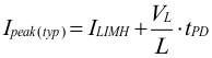
where
- ILIMH is the static current limit, as specified in the electrical characteristics
- L is the effective inductance (typically 470 nH)
- VL is the voltage across the inductor (VIN - VOUT)
- tPD is the internal propagation delay of typically 50 ns
The dynamic peak current is calculated as follows:
Equation 8. 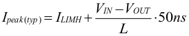
The low-side MOSFET also contains a negative current limit to prevent excessive current from flowing back through the inductor to the input. If the low-side sinking current limit is exceeded, the low-side MOSFET is turned off. In this scenario, both MOSFETs are off until the start of the next cycle. The negative current limit is only active in Forced PWM mode.