JAJSMX6C october 2022 – july 2023 TPSM82912 , TPSM82913 , TPSM82913E
PRODUCTION DATA
- 1
- 1 特長
- 2 アプリケーション
- 3 概要
- 4 Revision History
- 5 Pin Configuration and Functions
- 6 Specifications
-
7 Detailed Description
- 7.1 Overview
- 7.2 Functional Block Diagram
- 7.3
Feature Description
- 7.3.1 Smart Config (S-CONF)
- 7.3.2 Device Enable (EN/SYNC)
- 7.3.3 Device Synchronization (EN/SYNC)
- 7.3.4 Spread Spectrum Modulation
- 7.3.5 Output Discharge
- 7.3.6 Undervoltage Lockout (UVLO)
- 7.3.7 Power-Good Output
- 7.3.8 Noise Reduction and Soft-Start Capacitor (NR/SS)
- 7.3.9 Current Limit and Short-Circuit Protection
- 7.3.10 Thermal Shutdown
- 7.4 Device Functional Modes
- 8 Application and Implementation
- 9 Device and Documentation Support
- 10Mechanical, Packaging, and Orderable Information
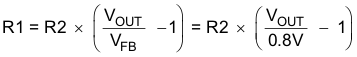
8.2.2.2.5 Setting the Output Voltage
Choose resistors R1 and R2 to set the output voltage within a range of 0.8 V to 5.5 V, according to Equation 6. To keep the feedback network robust from noise, and to reduce the self-generated noise of resistors, set R2 equal to or lower than 5 kΩ. Lower values of FB resistors achieve better noise immunity, and lower light load efficiency, as explained in the Design Considerations for a Resistive Feedback Divider in a DC/DC Converter technical brief.
A feedforward capacitor (CFF) is not required for proper operation, but can further improve output noise. However, care must be taken in choosing the CFF, because the power-good (PG) function can not be valid with a large CFF during start-up, and can cause spurious triggering of the PG pin during a large load transient. Refer to the Pros and Cons Using a Feedforward Capacitor with a Low Dropout Regulator application report for a discussion of the pros and cons of using a feedforward capacitor.