SCDS208B JUNE 2007 – October 2016 TS3A24157
PRODUCTION DATA.
- 1 Features
- 2 Applications
- 3 Description
- 4 Revision History
- 5 Pin Configuration and Functions
- 6 Specifications
- 7 Parameter Measurement Information
- 8 Detailed Description
- 9 Application and Implementation
- 10Power Supply Recommendations
- 11Layout
- 12Device and Documentation Support
- 13Mechanical, Packaging, and Orderable Information
パッケージ・オプション
デバイスごとのパッケージ図は、PDF版データシートをご参照ください。
メカニカル・データ(パッケージ|ピン)
- RSE|10
- DGS|10
サーマルパッド・メカニカル・データ
発注情報
9 Application and Implementation
NOTE
Information in the following applications sections is not part of the TI component specification, and TI does not warrant its accuracy or completeness. TI’s customers are responsible for determining suitability of components for their purposes. Customers should validate and test their design implementation to confirm system functionality.
9.1 Application Information
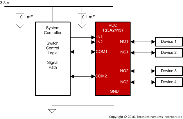
The switches are bidirectional, so the NO, NC, and COM pins can be used as either inputs or outputs.
9.2 Typical Application
 Figure 21. Typical Application Schematic
9.2.1 Design Requirements
The TS3A24157 can be properly operated without any external components.
When unused, pins COM, NC, and NO may be left floating.
Digital control pins IN must be pulled up to VCC or down to GND to avoid undesired switch positions that could result from the floating pin.
9.2.2 Detailed Design Procedure
Ensure that all of the signals passing through the switch are within the ranges specified in Recommended Operating Conditions to ensure proper performance.
9.2.3 Application Curves

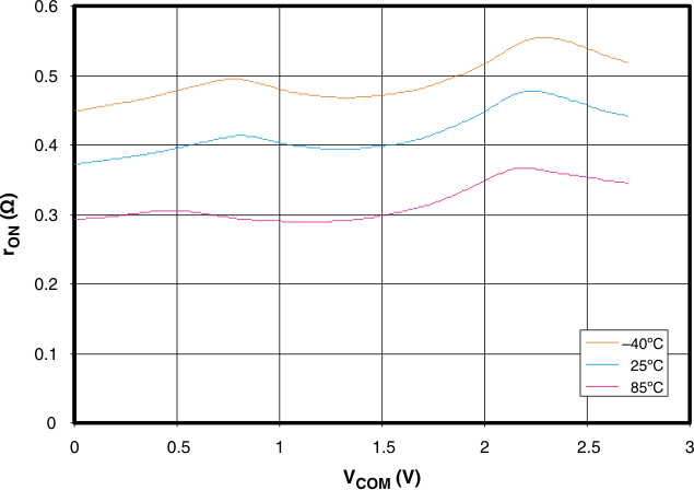
| VCC = 2.7 V |