JAJSM20A December 2020 – May 2021 TS3DV642-Q1
PRODUCTION DATA
- 1 特長
- 2 アプリケーション
- 3 概要
- 4 Revision History
- 5 Pin Configuration and Functions
- 6 Specifications
- 7 Parameter Measurement Information
- 8 Detailed Description
- 9 Application and Implementation
- 10Power Supply Recommendations
- 11Layout
- 12Device and Documentation Support
- 13Mechanical, Packaging, and Orderable Information
パッケージ・オプション
デバイスごとのパッケージ図は、PDF版データシートをご参照ください。
メカニカル・データ(パッケージ|ピン)
- RUA|42
サーマルパッド・メカニカル・データ
発注情報
9.3 Typical Application - Multiplexing HDMI Signals
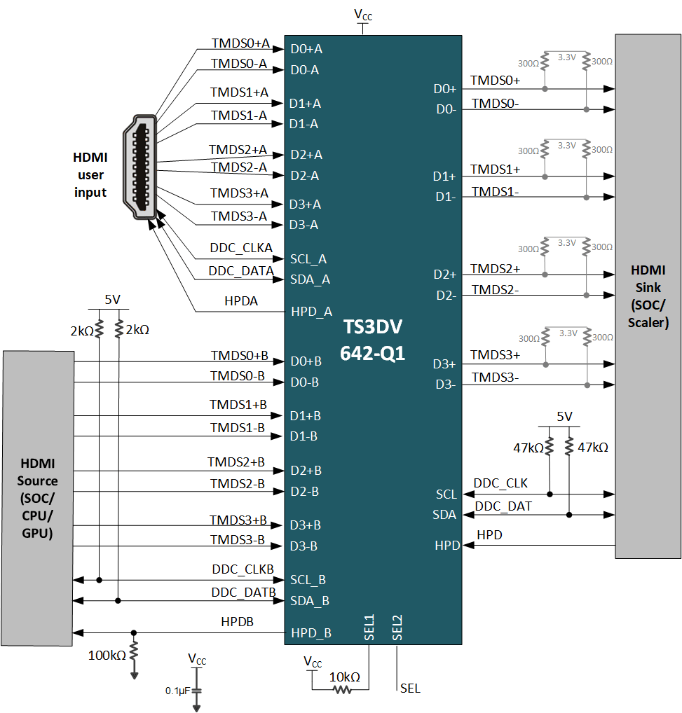
#FIG_X1Q_GV1_RPB shows a 2:1 multiplexing use case where TS3DV642-Q1 is being used to choose HDMI signals from either an external HDMI connector or an internal HDMI source to connect to a HDMI sink device. Note HDMI connector in this use case represents a Sink port and is subject to HDMI sink compliance requirements. Part of the compliance requirements the mainlink data and clock signals needs to have 50Ω termination from each pin to 3.3 V supply with certain tolerance depending on data rate. Note the TS3DV642-Q1 adds a series resistance (RON) to the mainlink sink termination. To account for the additional series resistance it is recommended that sink internal termination resistance is reduce by equal amount. Where such provisioning is not possibble, alternate solution is to install external resistors on board from each pin to VCC as shown in #FIG_X1Q_GV1_RPB. In applications where a retimer is used behind a HDMI connector in sink application, this series resistance provisioning is not required as retimer termination is tested for HDMI compliance.
 Figure 9-4 Multiplexing HDMI signals -
schematic