SLLSEL4A September 2014 – October 2014 TUSB1210-Q1
PRODUCTION DATA.
- 1 Features
- 2 Applications
- 3 Description
- 4 Revision History
- 5 Pin Configuration and Functions
-
6 Specifications
- 6.1 Absolute Maximum Ratings
- 6.2 Handling Ratings
- 6.3 Recommended Operating Conditions
- 6.4 Thermal Information
- 6.5 Analog I/O Electrical Characteristics
- 6.6 Digital I/O Electrical Characteristics
- 6.7 Digital IO Pins (Non-ULPI)
- 6.8 PHY Electrical Characteristics
- 6.9 Pullup/Pulldown Resistors
- 6.10 OTG Electrical Characteristics
- 6.11 Power Characteristics
- 6.12 Switching Characteristics
- 6.13 Timing Requirements
- 6.14 Typical Characteristics
-
7 Detailed Description
- 7.1 Overview
- 7.2 Functional Block Diagram
- 7.3 Feature Description
- 7.4 Device Functional Modes
- 7.5
Register Map
- 7.5.1 VENDOR_ID_LO
- 7.5.2 VENDOR_ID_HI
- 7.5.3 PRODUCT_ID_LO
- 7.5.4 PRODUCT_ID_HI
- 7.5.5 FUNC_CTRL
- 7.5.6 FUNC_CTRL_SET
- 7.5.7 FUNC_CTRL_CLR
- 7.5.8 IFC_CTRL
- 7.5.9 IFC_CTRL_SET
- 7.5.10 IFC_CTRL_CLR
- 7.5.11 OTG_CTRL
- 7.5.12 OTG_CTRL_SET
- 7.5.13 OTG_CTRL_CLR
- 7.5.14 USB_INT_EN_RISE
- 7.5.15 USB_INT_EN_RISE_SET
- 7.5.16 USB_INT_EN_RISE_CLR
- 7.5.17 USB_INT_EN_FALL
- 7.5.18 USB_INT_EN_FALL_SET
- 7.5.19 USB_INT_EN_FALL_CLR
- 7.5.20 USB_INT_STS
- 7.5.21 USB_INT_LATCH
- 7.5.22 DEBUG
- 7.5.23 SCRATCH_REG
- 7.5.24 SCRATCH_REG_SET
- 7.5.25 SCRATCH_REG_CLR
- 7.5.26 VENDOR_SPECIFIC1
- 7.5.27 VENDOR_SPECIFIC1_SET
- 7.5.28 VENDOR_SPECIFIC1_CLR
- 7.5.29 VENDOR_SPECIFIC2
- 7.5.30 VENDOR_SPECIFIC2_SET
- 7.5.31 VENDOR_SPECIFIC2_CLR
- 7.5.32 VENDOR_SPECIFIC1_STS
- 7.5.33 VENDOR_SPECIFIC1_LATCH
- 7.5.34 VENDOR_SPECIFIC3
- 7.5.35 VENDOR_SPECIFIC3_SET
- 7.5.36 VENDOR_SPECIFIC3_CLR
- 8 Application and Implementation
- 9 Power Supply Recommendations
- 10Layout
- 11Device and Documentation Support
- 12Mechanical, Packaging, and Orderable Information
パッケージ・オプション
メカニカル・データ(パッケージ|ピン)
- RHB|32
サーマルパッド・メカニカル・データ
- RHB|32
発注情報
8 Application and Implementation
NOTE
Information in the following applications sections is not part of the TI component specification, and TI does not warrant its accuracy or completeness. TI’s customers are responsible for determining suitability of components for their purposes. Customers should validate and test their design implementation to confirm system functionality.
8.1 Application Information
Figure 5 shows the suggested application diagram (Host or OTG, ULPI input-clock mode).
8.2 Typical Application
8.2.1 Host or OTG, ULPI Input Clock Mode Application
Figure 5 shows a suggested application diagram for TUSB1210-Q1 in the case of ULPI input-clock mode (60 MHz ULPI clock is provided by link processor), in Host or OTG application. Note this is just one example, it is of course possible to operate as HOST or OTG while also in ULPI output-clock mode.

8.2.1.1 Design Requirements
Table 9. Design Parameters
| DESIGN PARAMETER | EXAMPLE VALUE |
|---|---|
| VBAT | 3.3 V |
| VDDIO | 1.8 V |
| VBUS | 5.0 V |
| USB Support | HS, FS, LS |
| USB On the Go (OTG) | Yes |
| Clock Sources | 60 MHz Clock |
8.2.1.2 Detailed Design Procedure
Connect the TUSB1210 device as is shown in Figure 5.
Follow the Board Guidelines of the Application Report, SWCA124.
8.2.1.2.1 Unused Pins Connection
- VBUS: Input. Recommended to tie to GND if unused. However leaving VBUS floating is also acceptable since internally there is an 80 kΩ resistance to ground.
- REFCLK: Input. If REFCLK is unused, and 60 MHz clock is provided by MODEM (60 MHz should be connected to CLOCK pin in this case) then tie REFCLK to GND.
- CFG: Tie to GND if REFCLK is 19.2MHz, or tie to VDDIO if REFCLK is 26 MHz. Tie to either GND or VDDIO (doesn't matter which) if REFCLK not used (i.e., ULPI input clock configuration).
8.2.1.3 Application Curve
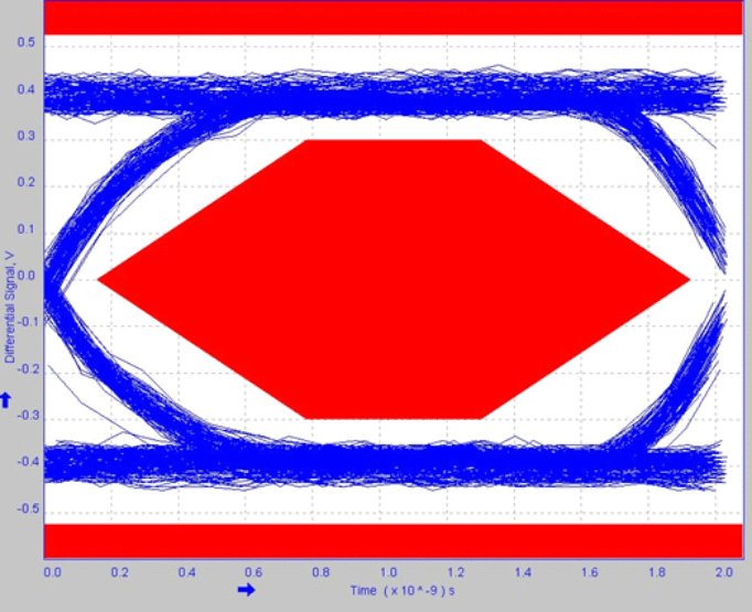 Figure 6. High-Speed Eye Diagram
8.2.2 Device, ULPI Output Clock Mode Application
Figure 7 shows a suggested application diagram for TUSB1210-Q1 in the case of ULPI output clock mode (60 MHz ULPI clock is provided by TUSB1210-Q1, while link processor or another external circuit provides REFCLK), in Device mode application. Note this is just one example, it is of course possible to operate as Device while also in ULPI input-clock mode. Refer also to Figure 5.

8.2.2.1 Design Requirements
Table 10. Design Parameters
| DESIGN PARAMETER | EXAMPLE VALUE |
|---|---|
| VBAT | 3.3 V |
| VDDIO | 1.8 V |
| VBUS | 5.0 V |
| USB Support | HS, FS, LS |
| Clock Sources | 26 MHz or 19.2 MHz Oscillator |
8.2.2.2 Detailed Design Procedure
Connect the TUSB1210 device as is shown in Figure 7.
Follow the Board Guidelines of the Application Report, SWCA124.
8.2.2.2.1 Unused Pins Connection
- ID: Input. Leave floating if unused or TUSB1210-Q1 is Device mode only. Tie to GND through RID < 1 kOhm if Host mode.
- REFCLK: Input. If REFCLK is unused, and 60 MHz clock is provided by MODEM (60 MHz should be connected to CLOCK pin in this case) then tie REFCLK to GND.
- CFG: Tie to GND if REFCLK is 19.2MHz, or tie to VDDIO if REFCLK is 26 MHz. Tie to either GND or VDDIO (doesn't matter which) if REFCLK not used (i.e., ULPI input clock configuration).
8.2.2.3 Application Curve
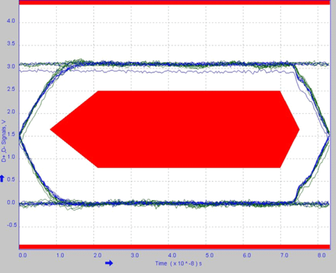 Figure 8. Full-Speed Eye Diagram
8.3 External Components
Table 11. TUSB1210-Q1 External Components
| FUNCTION | COMPONENT | REFERENCE | VALUE | NOTE | LINK |
|---|---|---|---|---|---|
| VDDIO | Capacitor | CVDDIO | 100 nF | Suggested value, application dependent | Figure 5 |
| VDD33 | Capacitor | CVDD33 | 2.2 μF | Range: [0.45 μF : 6.5 μF] , ESR = [0 : 600 mΩ] for f> 10 kHz |
Figure 5 |
| VDD15 | Capacitor | CVDD15 | 2.2 μF | Range: [0.45 μF : 6.5 μF] , ESR = [0 : 600 mΩ] for f> 10 kHz |
Figure 5 |
| VDD18 | Capacitor | Ext 1.8V supply | 100 nF | Suggested value, application dependent | Figure 5 |
| CVDD18 | |||||
| VBAT | Capacitor | CBYP | 100 nF(1) | Range: [0.45 μF : 6.5 μF] , ESR = [0 : 600 mΩ] for f> 10 kHz |
Figure 5 |
| VBUS | Capacitor | CVBUS | See Table 12 | Place close to USB connector | Figure 5 |