SLLSEL4A September 2014 – October 2014 TUSB1210-Q1
PRODUCTION DATA.
- 1 Features
- 2 Applications
- 3 Description
- 4 Revision History
- 5 Pin Configuration and Functions
-
6 Specifications
- 6.1 Absolute Maximum Ratings
- 6.2 Handling Ratings
- 6.3 Recommended Operating Conditions
- 6.4 Thermal Information
- 6.5 Analog I/O Electrical Characteristics
- 6.6 Digital I/O Electrical Characteristics
- 6.7 Digital IO Pins (Non-ULPI)
- 6.8 PHY Electrical Characteristics
- 6.9 Pullup/Pulldown Resistors
- 6.10 OTG Electrical Characteristics
- 6.11 Power Characteristics
- 6.12 Switching Characteristics
- 6.13 Timing Requirements
- 6.14 Typical Characteristics
-
7 Detailed Description
- 7.1 Overview
- 7.2 Functional Block Diagram
- 7.3 Feature Description
- 7.4 Device Functional Modes
- 7.5
Register Map
- 7.5.1 VENDOR_ID_LO
- 7.5.2 VENDOR_ID_HI
- 7.5.3 PRODUCT_ID_LO
- 7.5.4 PRODUCT_ID_HI
- 7.5.5 FUNC_CTRL
- 7.5.6 FUNC_CTRL_SET
- 7.5.7 FUNC_CTRL_CLR
- 7.5.8 IFC_CTRL
- 7.5.9 IFC_CTRL_SET
- 7.5.10 IFC_CTRL_CLR
- 7.5.11 OTG_CTRL
- 7.5.12 OTG_CTRL_SET
- 7.5.13 OTG_CTRL_CLR
- 7.5.14 USB_INT_EN_RISE
- 7.5.15 USB_INT_EN_RISE_SET
- 7.5.16 USB_INT_EN_RISE_CLR
- 7.5.17 USB_INT_EN_FALL
- 7.5.18 USB_INT_EN_FALL_SET
- 7.5.19 USB_INT_EN_FALL_CLR
- 7.5.20 USB_INT_STS
- 7.5.21 USB_INT_LATCH
- 7.5.22 DEBUG
- 7.5.23 SCRATCH_REG
- 7.5.24 SCRATCH_REG_SET
- 7.5.25 SCRATCH_REG_CLR
- 7.5.26 VENDOR_SPECIFIC1
- 7.5.27 VENDOR_SPECIFIC1_SET
- 7.5.28 VENDOR_SPECIFIC1_CLR
- 7.5.29 VENDOR_SPECIFIC2
- 7.5.30 VENDOR_SPECIFIC2_SET
- 7.5.31 VENDOR_SPECIFIC2_CLR
- 7.5.32 VENDOR_SPECIFIC1_STS
- 7.5.33 VENDOR_SPECIFIC1_LATCH
- 7.5.34 VENDOR_SPECIFIC3
- 7.5.35 VENDOR_SPECIFIC3_SET
- 7.5.36 VENDOR_SPECIFIC3_CLR
- 8 Application and Implementation
- 9 Power Supply Recommendations
- 10Layout
- 11Device and Documentation Support
- 12Mechanical, Packaging, and Orderable Information
パッケージ・オプション
メカニカル・データ(パッケージ|ピン)
- RHB|32
サーマルパッド・メカニカル・データ
- RHB|32
発注情報
6 Specifications
6.1 Absolute Maximum Ratings
over operating free-air temperature range (unless otherwise noted)(1)| MIN | MAX | UNIT | |||
|---|---|---|---|---|---|
| VCC | Main battery supply voltage (2) | 0 | 5 | V | |
| Voltage on any input(3) | Where supply represents the voltage applied to the power supply pin associated with the input | –0.3 | 1 × VCC +0.3 | V | |
| VBUS input | –2 | 20 | V | ||
| ID, DP, DM inputs | Stress condition specified 24h | –0.3 | 5.25 | V | |
| VDDIO | IO supply voltage | Continuous | –0.3 | 1.98 | V |
| TA | Ambient temperature range | –40 | 85 | °C | |
| TJ | Junction temperature range | –40 | 150 | °C | |
| Ambient temperature for parametric compliance | Parametric compliance | –14 | 125 | °C | |
| With max 125°C as junction temperature | –40 | 85 | °C | ||
| DP, DM, ID high voltage short circuit | DP, DM or ID pins short circuited to VBUS supply, in any mode of TUSB1210-Q1 operation, continuously for 24 hours | 0 | 5.25 | V | |
(1) Stresses beyond those listed under Absolute Maximum Ratings may cause permanent damage to the device. These are stress ratings only, and functional operation of the device at these or any other conditions beyond those indicated under Recommended Operating Conditions is not implied. Exposure to absolute-maximum-rated conditions for extended periods may affect device reliability.
(2) The product will have negligible reliability impact if voltage spikes of 5.5 V occur for a total (cumulative over lifetime) duration of 5 milliseconds.
(3) Except VBAT input, VBUS, ID, DP, and DM pads
6.2 Handling Ratings
| MIN | MAX | UNIT | ||||
|---|---|---|---|---|---|---|
| Tstg | Storage temperature range | –65 | 150 | °C | ||
| VESD | Electrostatic discharge (ESD) performance: | Human body model (HBM), per AEC Q100-002 Classification Level H1C, all pins(1) | 1500 | 1500 | V | |
| Charged device model (CDM), per AEC Q100-011 Classification Level C4B | Corner pins | –750 | 750 | |||
| Other pins | –500 | 500 | ||||
(1) AEC Q100-002 indicates HBM stressing is done in accordance with ANSI/ESDA/JEDEC JS-001 specifications.
6.3 Recommended Operating Conditions
over operating free-air temperature range (unless otherwise noted)6.4 Thermal Information
| THERMAL METRIC(1) | RHB | UNIT | ||
|---|---|---|---|---|
| (16 Pins) | ||||
| RθJA | Junction-to-ambient thermal resistance | 34.72 | °C/W | |
| RθJC(top) | Junction-to-case(top) thermal resistance | 37.3 | ||
| RθJB | Junction-to-board thermal resistance | 10.3 | ||
| ψJT | Junction-to-top characterization parameter | 0.5 | ||
| ψJB | Junction-to-board characterization parameter | 10.5 | ||
| RθJC(bottom) | Junction-to-case(bottom) thermal resistance | 3.6 | ||
(1) For more information about traditional and new thermal metrics, see the IC Package Thermal Metrics application report, SPRA953.
6.5 Analog I/O Electrical Characteristics
over operating free-air temperature range (unless otherwise noted)| PARAMETER | CONDITIONS | MIN | TYP | MAX | UNIT | |
|---|---|---|---|---|---|---|
| CPEN Output Pin | ||||||
| VOL | CPEN low-level output voltage | IOL = 3 mA | 0.3 | V | ||
| VOH | CPEN high-level output voltage | IOH = –3 mA | VDD33 – 0.3 | V | ||
6.6 Digital I/O Electrical Characteristics
over operating free-air temperature range (unless otherwise noted)| PARAMETER | TEST CONDITIONS | MIN | TYP | MAX | UNIT | |
|---|---|---|---|---|---|---|
| CLOCK | ||||||
| VOL | Low-level output voltage | Frequency = 60 MHz, Load = 10 pF | 0.45 | V | ||
| VOH | High-level output voltage | VDDIO - 0.45 | V | |||
| STP, DIR, NXT, DATA0 to DATA7 | ||||||
| VOL | Low-level output voltage | Frequency = 30 MHz, Load = 10 pF | 0.45 | |||
| VOH | High-level output voltage | VDDIO - 0.45 | ||||
6.7 Digital IO Pins (Non-ULPI)
over operating free-air temperature range (unless otherwise noted)| PARAMETER | TEST CONDITIONS | MIN | TYP | MAX | UNIT | |
|---|---|---|---|---|---|---|
| CS, CFG, RESETB Input Pins | ||||||
| VIL | Maximum low-level input voltage | 0.35 x VDDIO | V | |||
| VIH | Minimum high-level input voltage | 0.65 x VDDIO | V | |||
| RESETB Input Pin Timing Spec | ||||||
| tw(POR) | Internal power-on reset pulse width | 0.2 | μs | |||
| tw(RESET) | External RESETB pulse width | Applied to external RESETB pin when CLOCK is toggling. | 8 | CLOCK cycles | ||
6.8 PHY Electrical Characteristics
over operating free-air temperature range (unless otherwise noted)| PARAMETER | COMMENTS | MIN | TYP | MAX | UNIT | ||
|---|---|---|---|---|---|---|---|
| LS/FS Single-Ended Receivers | |||||||
| USB single-ended receivers | |||||||
| SKWVP_VM | Skew between VP and VM | Driver outputs unloaded | –2 | 0 | 2 | ns | |
| VSE_HYS | Single-ended hysteresis | 50 | mV | ||||
| VIH | High (driven) | 2 | V | ||||
| VIL | Low | 0.8 | V | ||||
| VTH | Switching threshold | 0.8 | 2 | V | |||
| LS/FS Differential Receiver | |||||||
| VDI | Differential input sensitivity | Ref. USB2.0 | 200 | mV | |||
| VCM | Differential Common mode range | Ref. USB2.0 | 0.8 | 2.5 | V | ||
| LS Transmitter | |||||||
| VOL | Low | Ref. USB2.0 | 0 | 300 | mV | ||
| VOH | High (driven) | Ref. USB2.0 | 2.8 | 3.6 | V | ||
| VCRS | Output signal crossover voltage | Ref. USB2.0, covered by eye diagram | 1.3 | 2 | V | ||
| tr | Rise time | Ref. USB2.0, covered by eye diagram | 75 | 300 | ns | ||
| tf | Fall time | 75 | 300 | ns | |||
| tFRFM | Differential rise and fall time matching | 80% | 125% | ||||
| tFDRATE | Low-speed data rate | Ref. USB2.0, covered by eye diagram | 1.4775 | 1.5225 | Mb/s | ||
| tDJ1 | Source jitter total (including frequency tolerance) | To next transition | Ref. USB2.0, covered by eye diagram | –25 | 25 | ns | |
| tDJ2 | For paired transitions | –10 | 10 | ||||
| tFEOPT | Source SE0 interval of EOP | Ref. USB2.0, covered by eye diagram | 1.25 | 1.5 | µs | ||
| Downstream eye diagram | Ref. USB2.0, covered by eye diagram | ||||||
| VCM | Differential common mode range | Ref. USB2.0 | 0.8 | 2.5 | V | ||
| FS Transmitter | |||||||
| VOL | Low | Ref. USB2.0 | 0 | 300 | mV | ||
| VOH | High (driven) | Ref. USB2.0 | 2.8 | 3.6 | V | ||
| VCRS | Output signal crossover voltage | Ref. USB2.0, covered by eye diagram | 1.3 | 2 | V | ||
| tFR | Rise time | Ref. USB2.0 | 4 | 20 | ns | ||
| tFF | Fall time | Ref. USB2.0 | 4 | 20 | ns | ||
| tFRFM | Differential rise and fall time matching | Ref. USB2.0, covered by eye diagram | 90% | 111.11% | |||
| ZDRV | Driver output resistance | Ref. USB2.0 | 28 | 44 | Ω | ||
| TFDRATE | Full-speed data rate | Ref. USB2.0, covered by eye diagram | 11.97 | 12.03 | Mb/s | ||
| tDJ1 | Source jitter total (including frequency tolerance) | To next transition | Ref. USB2.0, covered by eye diagram | –2 | 2 | ns | |
| tDJ2 | For paired transitions | –1 | 1 | ||||
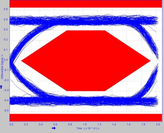
| TFEOPT | Source SE0 interval of EOP | Ref. USB2.0, covered by eye diagram | 160 | 175 | ns | ||
| Downstream eye diagram | Ref. USB2.0, covered by eye diagram | ||||||
| Upstream eye diagram | |||||||
| HS Differential Receiver | |||||||
| VHSSQ | High-speed squelch detection threshold (differential signal amplitude) | Ref. USB2.0 | 100 | 150 | mV | ||
| VHSDSC | High-speed disconnect detection threshold (differential signal amplitude) | Ref. USB2.0 | 525 | 625 | mV | ||
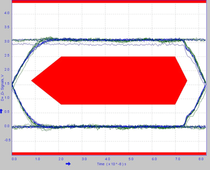
| High-speed differential input signaling levels | Ref. USB2.0, specified by eye pattern templates | mV | |||||
| VHSCM | High-speed data signaling common mode voltage range (guidelines for receiver) | Ref. USB2.0 | –50 | 500 | mV | ||
| Receiver jitter tolerance | Ref. USB2.0, specified by eye pattern templates | 150 | ps | ||||
| HS Transmitter | |||||||
| VHSOI | High-speed idle level | Ref. USB2.0 | –10 | 10 | mV | ||
| VHSOH | High-speed data signaling high | Ref. USB2.0 | 360 | 440 | mV | ||
| VHSOL | High-speed data signaling low | Ref. USB2.0 | –10 | 10 | mV | ||
| VCHIRPJ | Chirp J level (differential voltage) | Ref. USB2.0 | 700 | 1100 | mV | ||
| VCHIRPK | Chirp K level (differential voltage) | Ref. USB2.0 | -900 | -500 | mV | ||
| tr | Rise Time (10% - 90%) | Ref. USB2.0, covered by eye diagram | 500 | ps | |||
| tf | Fall time (10% - 90%) | Ref. USB2.0, covered by eye diagram | 500 | ps | |||
| ZHSDRV | Driver output resistance (which also serves as high-speed termination) | Ref. USB2.0 | 40.5 | 49.5 | Ω | ||
| THSDRAT | High-speed data range | Ref. USB2.0, covered by eye diagram | 479.76 | 480.24 | Mb/s | ||
| Data source jitter | Ref. USB2.0, covered by eye diagram | ||||||
| Downstream eye diagram | Ref. USB2.0, covered by eye diagram | ||||||
| Upstream eye diagram | Ref. USB2.0, covered by eye diagram | ||||||
| CEA-2011/UART Transceiver | |||||||
| UART Transmitter CEA-2011 | |||||||
| tPH_UART_EDGE | Phone UART edge rates | DP_PULLDOWN asserted | 1 | Μs | |||
| VOH_SER | Serial interface output high | ISOURCE = 4 mA | 2.4 | 3.3 | 3.6 | V | |
| VOL_SER | Serial interface output low | ISINK = –4 mA | 0 | 0.1 | 0.4 | V | |
| UART Receiver CEA-2011 | |||||||
| VIH_SER | Serial interface input high | DP_PULLDOWN asserted | 2 | V | |||
| VIL_SER | Serial interface input low | DP_PULLDOWN asserted | 0.8 | V | |||
| VTH | Switching threshold | 0.8 | 2 | V | |||
6.9 Pullup/Pulldown Resistors
over operating free-air temperature range (unless otherwise noted)| PARAMETER | COMMENTS | MIN | TYP | MAX | UNIT | |
|---|---|---|---|---|---|---|
| RPUI | Bus pullup resistor on upstream port (idle bus) | Bus idle | 0.9 | 1.1 | 1.575 | kΩ |
| RPUA | Bus pullup resistor on upstream port (receiving) | Bus driven/driver's outputs unloaded | 1.425 | 2.2 | 3.09 | |
| VIHZ | High (floating) | Pullups/pulldowns on both DP and DM lines | 2.7 | 3.6 | V | |
| VPH_DP_UP | Phone D+ pullup voltage | Driver's outputs unloaded | 3 | 3.3 | 3.6 | V |
| Pulldown resistors | ||||||
| RPH_DP_DWN | Phone D+/– pulldown | Driver's outputs unloaded | 14.25 | 18 | 24.8 | kΩ |
| RPH_DM_DWN | ||||||
| VIHZ | High (floating) | Pullups/pulldowns on both DP and DM lines | 2.7 | 3.6 | V | |
| D+/– Data line | ||||||
| CINUB | Upstream facing port | [1.0] | 22 | 75 | pF | |
| VOTG_DATA_LKG | On-the-go device leakage | [2] | 0.342 | V | ||
| ZINP | Input impedance exclusive of pullup/pulldown | Driver's outputs unloaded | 300 | kΩ | ||
6.10 OTG Electrical Characteristics
over operating free-air temperature range (unless otherwise noted)| PARAMETER | COMMENTS | MIN | TYP | MAX | UNIT | ||
|---|---|---|---|---|---|---|---|
| OTG VBUS Electrical | |||||||
| VBUS Comparators | |||||||
| VA_SESS_VLD | A-device session valid | 0.8 | 1.4 | 2.0 | V | ||
| VA_VBUS_VLD | A-device VBUS valid | 4.4 | 4.5 | 4.625 | V | ||
| VB_SESS_END | B-device session end | 0.2 | 0.5 | 0.8 | V | ||
| VB_SESS_VLD | B-device session valid | 2.1 | 2.4 | 2.7 | V | ||
| VBUS Line | |||||||
| RA_BUS_IN | A-device VBUS input impedance to ground | SRP (VBUS pulsing) capable A-device not driving VBUS | 40 | 70 | 100 | kΩ | |
| RB_SRP_DWN | B-device VBUS SRP pulldown | 5.25 V / 8 mA, Pullup voltage = 3 V | 0.656 | 10 | kΩ | ||
| RB_SRP_UP | B-device VBUS SRP pullup | (5.25 V – 3 V) / 8 mA, Pullup voltage = 3 V | 0.281 | 1 | 2 | kΩ | |
| tRISE_SRP_UP_MAX | B-device VBUS SRP rise time maximum for OTG-A communication | 0 to 2.1 V with < 13 μF load | RVBUS = 0 Ω and R1KSERIES = '0' |
31.4 | ms | ||
| RVBUS = 1000 Ω ±10% and R1KSERIES = '1' |
57.8 | ||||||
| RVBUS = 1200 Ω ±10% and R1KSERIES = '1' |
64 | ||||||
| RVBUS = 1800 Ω ±10% and R1KSERIES = '1' |
85.4 | ||||||
| tRISE_SRP_UP_MIN | B-device VBUS SRP rise time minimum for standard host connection | 0.8 to 2 V with > 97 μF load | RVBUS = 0 Ω and R1KSERIES = '0' |
46.2 | ms | ||
| RVBUS = 1000 Ω ±10% and R1KSERIES = '1' |
96 | ||||||
| RVBUS = 1200 Ω ±10% and R1KSERIES = '1' |
100 | ||||||
| RVBUS = 1800 Ω ±10% and R1KSERIES = '1' |
100 | ||||||
Table 1. OTG ID Electrical
| PARAMETER | COMMENTS | MIN | TYP | MAX | UNIT | ||
|---|---|---|---|---|---|---|---|
| ID Comparators — ID External Resistors Specifications | |||||||
| RID_GND | ID ground comparator | ID_GND interrupt | 12 | 20 | 28 | kΩ | |
| RID_FLOAT | ID Float comparator | ID_FLOAT interrupt | 200 | 500 | kΩ | ||
| ID Line | |||||||
| RPH_ID_UP | Phone ID pullup to VPH_ID_UP | ID unloaded (VRUSB) | 70 | 90 | 286 | kΩ | |
| VPH_ID_UP | Phone ID pullup voltage | Connected to VRUSB | 2.5 | 3.2 | V | ||
| ID line maximum voltage | 5.25 | V | |||||
6.11 Power Characteristics
over operating free-air temperature range (unless otherwise noted)| PARAMETER | TEST CONDITIONS | MIN | TYP | MAX | UNIT | ||
|---|---|---|---|---|---|---|---|
| VDD33 Internal LDO Regulator Characteristics | |||||||
| VINVDD33 | Input voltage | VBAT USB | VVDD33 typ + 0.2 | 3.6 | 4.5 | V | |
| VVDD33 | Output voltage | ON mode, | VUSB3V3_VSEL = ‘000 | 2.4 | 2.5 | 2.6 | V |
| VUSB3V3_VSEL = ‘001 | 2.65 | 2.75 | 2.85 | ||||
| VUSB3V3_VSEL = ‘010 | 2.9 | 3.0 | 3.1 | ||||
| VUSB3V3_VSEL = ‘011 (default) | 3.0 | 3.1 | 3.2 | ||||
| VUSB3V3_VSEL = ‘100 | 3.1 | 3.2 | 3.3 | ||||
| VUSB3V3_VSEL = ‘101 | 3.2 | 3.3 | 3.4 | ||||
| VUSB3V3_VSEL = ‘110 | 3.3 | 3.4 | 3.5 | ||||
| VUSB3V3_VSEL = ‘111 | 3.4 | 3.5 | 3.6 | ||||
| IVDD33 | Rated output current | VBAT USB | Active mode | 15 | mA | ||
| Suspend/reset mode | 1 | ||||||
| VDD15 Internal LDO Regulator Characteristics | |||||||
| VIN VDD15 | Input voltage | On mode, VIN VDD15 = VBAT | 2.7 | 3.6 | 4.5 | V | |
| VVDD15 | Output voltage | VINVDD15 min – VINVDD15 max | 1.45 | 1.56 | 1.65 | V | |
| IVDD15 | Rated output current | On mode | 30 | mA | |||
6.12 Switching Characteristics
over operating free-air temperature range (unless otherwise noted)| PARAMETER | TEST CONDITIONS | MIN | TYP | MAX | UNIT | |
|---|---|---|---|---|---|---|
| Electrical Characteristics: Clock Input | ||||||
| Clock input duty cycle | 40 | 60% | ||||
| fCLK | Clock nominal frequency | 60 | MHz | |||
| Clock input rise/fall time | In % of clock period tCLK ( = 1/fCLK ) | 10% | ||||
| Clock input frequency accuracy | 250 | ppm | ||||
| Clock input integrated jitter | 600 | ps rms | ||||
| Electrical Characteristics: REFCLK | ||||||
| REFCLK input duty cycle | 40 | 60% | ||||
| fREFCLK | REFCLK nominal frequency | When CFG pin is tied to GND | 19.2 | MHz | ||
| When CFG pin is tied to VDDIO | 26 | |||||
| REFCLK input rise/fall time | In % of clock period tREFCLK ( = 1/fREFCLK ) | 20% | ||||
| REFCLK input frequency accuracy | 250 | ppm | ||||
| REFCLK input integrated jitter | 600 | ps rms | ||||
| REFCLK HIZ Leakage current | 3 | µA | ||||
| REFCLK HIZ Leakage current | –3 | |||||
| Digital IO Electrical Characteristics: CLOCK | ||||||
| tr | Rise time | Frequency = 60 MHz, Load = 10 pF | 1 | ns | ||
| tf | Fall time | Frequency = 30 MHz, Load = 10 pF | 1 | ns | ||
| Digital IO Electrical Characteristics: STP, DIR, NXT, DATA0 to DATA7 | ||||||
| tr | Rise time | Frequency = 30 MHz, Load = 10 pF | 1 | ns | ||
| tf | Fall time | 1 | ns | |||
6.13 Timing Requirements
| PARAMETER | INPUT CLOCK | OUTPUT CLOCK | UNIT | |||
|---|---|---|---|---|---|---|
| MIN | MAX | MIN | MAX | |||
| ULPI Interface Timing | ||||||
| tSC, tSD | Set-up time (control in, 8-bit data in) | 3 | 6 | ns | ||
| tSC, tHD | Hold time (control in, 8-bit data in) | 1.5 | 0 | ns | ||
| tDC, tDD | Output delay (control out, 8-bit data out) | 6 | 9 | ns | ||
| USB UART Interface Timing | ||||||
| tPH_DP_CON | Phone D+ connect time | 100 | ms | |||
| tPH_DISC_DET | Phone D+ disconnect time | 150 | ms | |||
| fUART_DFLT | Default UART signaling rate (typical rate) | 9600 | bps | |||
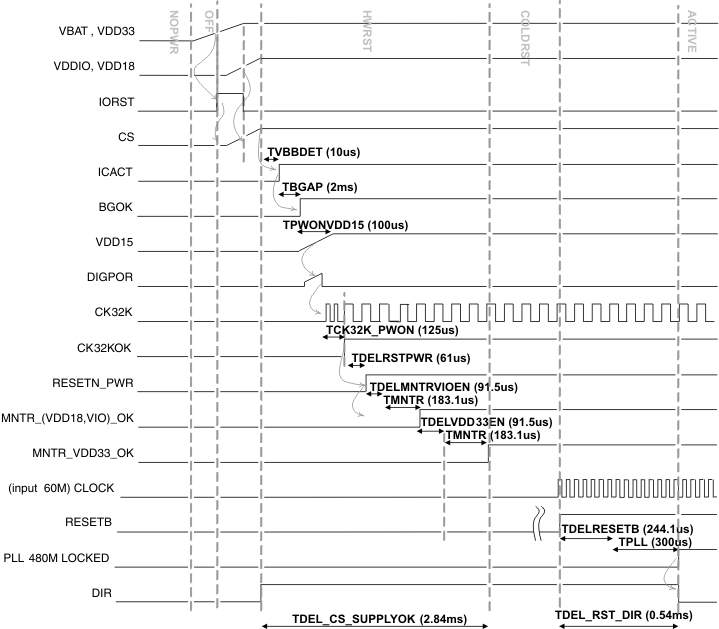 Figure 1. TUSB1210-Q1 Power-Up Timing (ULPI Clock Input Mode)
Table 2. Timers and Debounce
| PARAMETER | COMMENTS | MIN | TYP | MAX | UNIT | |
|---|---|---|---|---|---|---|
| tDEL_CS_SUPPLYOK | Chip-select-to-supplies OK delay | 2.84 | 4.10 | ms | ||
| tDEL_RST_DIR | RESETB to PHY PLL locked and DIR falling-edge delay | 0.54 | 0.647 | ms | ||
| tVBBDET | VBAT detection delay | 10 | µs | |||
| tBGAP | Bandgap power-on delay | 2 | ms | |||
| tPWONVDD15 | VDD15 power-on delay | 100 | µs | |||
| tPWONCK32K | 32-KHz RC-OSC power-on delay | 125 | µs | |||
| tDELRSTPWR | Power control reset delay | 61 | µs | |||
| tDELMNTRVIOEN | Monitor enable delay | 91.5 | µs | |||
| tMNTR | Supply monitoring debounce | 183.1 | µs | |||
| tDELVDD33EN | VDD33 LDO enable delay | 93.75 | µs | |||
| tDELRESETB | RESETB internal delay | 244.1 | µs | |||
| tPLL | PLL lock time | 300 | µs | |||
6.13.1 Timing Parameter Definitions
The timing parameter symbols used in the timing requirement and switching characteristic tables are created in accordance with JEDEC Standard 100. To shorten the symbols, some pin names and other related terminologies have been abbreviated as shown in Table 3.
Table 3. Timing Parameter Definitions
| LOWERCASE SUBSCRIPTS | |
|---|---|
| SYMBOL | PARAMETER |
| C | Cycle time (period) |
| D | Delay time |
| Dis | Disable time |
| En | Enable time |
| H | Hold time |
| Su | Setup time |
| START | Start bit |
| T | Transition time |
| V | Valid time |
| W | Pulse duration (width) |
| X | Unknown, changing, or don't care level |
| H | High |
| L | Low |
| V | Valid |
| IV | Invalid |
| AE | Active edge |
| FE | First edge |
| LE | Last edge |
| Z | High impedance |
6.13.2 Interface Target Frequencies
Table 4 assumes testing over the recommended operating conditions.
Table 4. TUSB1210-Q1 Interface Target Frequencies
| IO INTERFACE |
INTERFACE DESIGNATION | TARGET FREQUENCY 1.5 V |
|
|---|---|---|---|
| USB | Universal serial bus | High speed | 480 Mbits/s |
| Full speed | 12 Mbits/s | ||
| Low speed | 1.5 Mbits/s | ||