SLLSEJ1A March 2014 – March 2014 TUSB551
PRODUCTION DATA.
- 1 Features
- 2 Applications
- 3 Description
- 4 Simplified Schematic
- 5 Revision History
- 6 Terminal Configuration and Functions
-
7 Specifications
- 7.1 Absolute Maximum Ratings
- 7.2 Handling Ratings
- 7.3 Recommended Operating Conditions
- 7.4 Thermal Information
- 7.5 Power Supply Electrical Characteristics
- 7.6 DC Electrical Characteristics
- 7.7 AC Electrical Characteristics
- 7.8 Timing Requirements/Timing Diagrams
- 7.9 Switching Characteristics
- 7.10 Typical Characteristics
- 8 Detailed Description
- 9 Applications and Implementation
- 10Power Supply Recommendations
- 11Layout
- 12Device and Documentation Support
- 13Mechanical, Packaging, and Orderable Information
9 Applications and Implementation
9.1 Application Information
One example of the TUSB551 used in a Host application on transmit and receive channels is shown below. The re-driver is needed on the transmit path to pass transmitter compliance due to loss between the Host and connector. The re-driver uses it’s equalization to recover the insertion loss and re-drive the signal with boosted swing down the remaining channel, through the USB3.0 cable, and into the device PCB. Additionally, the TUSB551 is needed on the receive channel for the Host to pass receiver jitter tolerance. The re-driver recovers the loss from the Device PCB, connector, and USB 3.0 cable and re-drives the signal going into the Host receiver. The equalization, output swing, and de-emphasis settings are dependent upon the type of USB3.0 signal path and end application.
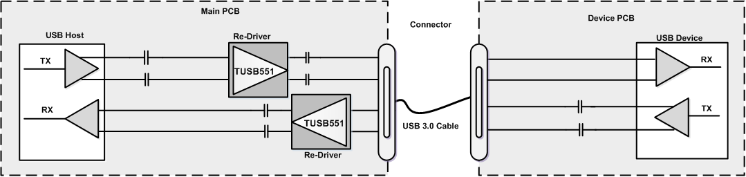 Figure 11. Application for Host Systems
9.2 Typical Application
9.2.1 Transmit and Receive Channels
The TUSB551 is placed in the transmitter channel and connected to a USB3 Type-A connector. This particular example shows the polarity swapped on the RXP/N and TXP/N differential pairs. The positive signal may be routed to RXN as long as the corresponding output, TXN, is routed to the positive terminal on the connector (SSTXP). This allows routing to be done without crossing the differential pair signals and using extra vias. The EQ and DE terminals must be pulled up, pulled down, or left floating depending on the amount of equalization or de-emphasis that is desired. The OS terminal must be pulled down or left floating depending on the required output swing. In this example, the EQ terminal is pulled low through a resistor and the OS and DE terminals are left floating.
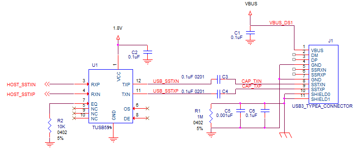 Figure 12. Transmitter Channel Implementation with Differential Pair Polarity Swapped
The TUSB551 is placed in the receiver channel and connected to a USB3 Type-A connector. This example shows the polarity matched, and the TUSB551 footprint is rotated so the trace routing of the differential pairs will not overlap. The EQ and DE terminals must be pulled up, pulled down, or left floating depending on the amount of equalization or de-emphasis that is desired. The OS terminal must be pulled down or left floating depending on the required output swing. In this example, the EQ and OS terminals are left floating and the DE terminal is pulled up through a resistor.
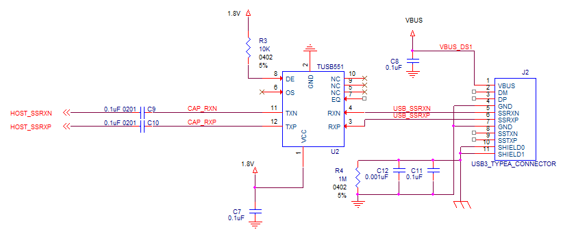 Figure 13. Receive Channel Implementation
9.2.1.1 Design Requirements
| DESIGN PARAMETER | EXAMPLE VALUE |
|---|---|
| Input Voltage Range | 100 mV to 1200 mV |
| Output Voltage Range | 1050 mV to 1200 mV |
| Equalization | 3, 6, 9 dB |
| De-Emphasis | 0, –3.5, –6 dB (OS Floating) |
| VCC | 1.8 V nominal supply |
9.2.1.2 Detailed Design Procedure
To begin the design process, determine the following:
- Equalization (EQ) setting
- De-Emphasis (DE) setting
- Output Swing Amplitude (OS) setting
The equalization should be set based on the insertion loss in the pre-channel (channel before the TUSB551 device). The input voltage to the device is able to have a large range because of the receiver sensitivity and the available EQ settings. The EQ terminal can be pulled high through a resistor to VCC, low through a resistor to ground, or left floating. The application schematic above shows the implementation. See Device Functional Modes section for EQ values.
The De-Emphasis setting should be set based on the length and characteristics of the post channel (channel after the TUSB551 device). Output de-emphasis can be tailored using the DE terminal. This terminal should be pulled high through a resistor to VCC, low through a resistor to ground, or left floating. The application schematic above shows the implementation. See Device Functional Modes section for DE values.
The output swing setting can also be configured based on the amplitude needed to pass the compliance test. This setting will also be based on the length of interconnect or cable the TUSB551 is driving. This terminal should be pulled low through a resistor to ground or left floating. The application schematic above shows the implementation. See Device Functional Modes section for OS values.
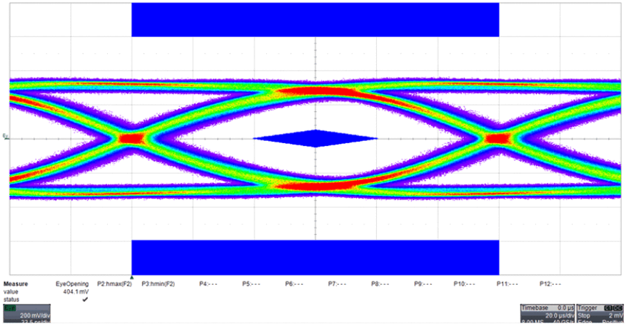
9.2.1.3 Application Performance Plot