JAJSLU9A May 2021 – November 2021 TXU0304
PRODUCTION DATA
- 1 特長
- 2 アプリケーション
- 3 概要
- 4 Revision History
- 5 Related Products
- 6 Pin Configuration and Functions—TXU0304
-
7 Specifications
- 7.1 Absolute Maximum Ratings
- 7.2 ESD Ratings
- 7.3 Recommended Operating Conditions
- 7.4 Thermal Information
- 7.5 Electrical Characteristics
- 7.6 Switching Characteristics: Tsk, TMAX
- 7.7 Switching Characteristics, VCCA = 1.2 ± 0.1 V
- 7.8 Switching Characteristics, VCCA = 1.5 ± 0.1 V
- 7.9 Switching Characteristics, VCCA = 1.8 ± 0.15 V
- 7.10 Switching Characteristics, VCCA = 2.5 ± 0.2 V
- 7.11 Switching Characteristics, VCCA = 3.3 ± 0.3 V
- 7.12 Switching Characteristics, VCCA = 5.0 ± 0.5 V
- 7.13 Operating Characteristics
- 7.14 Typical Characteristics
- 8 Parameter Measurement Information
-
9 Detailed Description
- 9.1 Overview
- 9.2 Functional Block Diagram
- 9.3
Feature Description
- 9.3.1 CMOS Schmitt-Trigger Inputs with Integrated Pulldowns
- 9.3.2 Control Logic (OE) with VCC(MIN) Circuitry
- 9.3.3 Balanced High-Drive CMOS Push-Pull Outputs
- 9.3.4 Partial Power Down (Ioff)
- 9.3.5 VCC Isolation and VCC Disconnect
- 9.3.6 Over-Voltage Tolerant Inputs
- 9.3.7 Glitch-Free Power Supply Sequencing
- 9.3.8 Negative Clamping Diodes
- 9.3.9 Fully Configurable Dual-Rail Design
- 9.3.10 Supports High-Speed Translation
- 9.4 Device Functional Modes
- 10Application and Implementation
- 11Power Supply Recommendations
- 12Layout
- 13Device and Documentation Support
- 14Mechanical, Packaging, and Orderable Information
パッケージ・オプション
メカニカル・データ(パッケージ|ピン)
サーマルパッド・メカニカル・データ
- BQA|14
発注情報
5 Related Products
- TXU0x04 4-Bit Unidirectional Voltage-Level TranslatorsTXU0x04 are 4-bit, dual-supply noninverting fixed direction voltage level translators. These devices are compatible to the TXB0104 with the same pinout allowing for a drop in replacement. The OE pin can be referenced to either VCCA or VCCB logic levels allowing for one of the TXU0x04 devices to be used for fixed direction, high drive applications which the TXB0104 is not recommended to support.
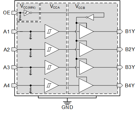
- TXU0104TXU0104 is a 4-bit, dual-supply noninverting fixed direction voltage level translators with all 4 channels in the same direction commonly used for GPIO translation.
 Figure 5-1 TXU0104 Functional Block Diagram
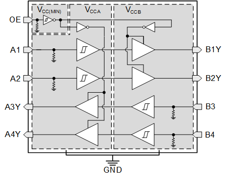
- TXU0204TXU0204 is a 4-bit, dual-supply noninverting fixed direction voltage level translators with 2 channels in the opposing direction commonly used for GPIO, UART, and JTAG translation.
 Figure 5-2 TXU0204 Functional Block Diagram