SCES959A December 2023 – April 2024 TXV0108
PRODUCTION DATA
- 1
- 1 Features
- 2 Applications
- 3 Description
- 4 Pin Configuration and Functions
-
5 Specifications
- 5.1 Absolute Maximum Ratings
- 5.2 ESD Ratings
- 5.3 Recommended Operating Conditions
- 5.4 Thermal Information
- 5.5 Electrical Characteristics
- 5.6 Switching Characteristics, VCCA = 1.2 ± 0.06 V
- 5.7 Switching Characteristics, VCCA = 1.8 ± 0.15 V
- 5.8 Switching Characteristics, VCCA = 2.5 ± 0.2 V
- 5.9 Switching Characteristics, VCCA = 3.3 ± 0.3 V
- 5.10 Typical Characteristics
- 6 Parameter Measurement Information
-
7 Detailed Description
- 7.1 Overview
- 7.2 Functional Block Diagram
- 7.3
Feature Description
- 7.3.1 Balanced High-Drive CMOS Push-Pull Outputs
- 7.3.2 Partial Power Down (Ioff)
- 7.3.3 VCC Isolation and VCC Disconnect (Ioff-float)
- 7.3.4 Over-Voltage Tolerant Inputs
- 7.3.5 Negative Clamping Diodes
- 7.3.6 Fully Configurable Dual-Rail Design
- 7.3.7 Supports Timing Sensitive Translation
- 7.3.8 Integrated Damping Resistor and Impedance Matching
- 7.4 Device Functional Modes
- 8 Application and Implementation
- 9 Device and Documentation Support
- 10Revision History
- 11Mechanical, Packaging, and Orderable Information
パッケージ・オプション
デバイスごとのパッケージ図は、PDF版データシートをご参照ください。
メカニカル・データ(パッケージ|ピン)
- RGY|24
サーマルパッド・メカニカル・データ
- RGY|24
発注情報
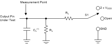
6.1 Load Circuit and Voltage Waveforms
Unless otherwise noted, all input pulses are supplied by generators having the following characteristics:
- f = 1MHz
- ZO = 50Ω
- Δt/ΔV ≤ 1ns/V

A. CL includes probe and jig capacitance.
Figure 6-1 Load CircuitTable 6-1 Load Circuit Conditions
| Parameter | VCCO | RL | CL | S1 | VTP | |
|---|---|---|---|---|---|---|
| tpd | Propagation (delay) time | 1.14V – 3.6V | 2kΩ | 15pF | Open | N/A |
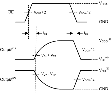
| ten, tdis | Enable time, disable time | 1.14V – 3.6V | 2kΩ | 15pF | 2 × VCCO | 0.15V |
| ten, tdis | Enable time, disable time | 1.14V – 3.6V | 2kΩ | 15pF | GND | 0.15V |

- The greater between tPLH and tPHL is the same as tpd.
- VOH and VOL are typical output voltage levels that occur with specified RL, CL, and S1

- VOH and VOL are typical output voltage levels that occur with specified RL, CL, and S1

A. Output waveform on the condition that input is driven to a valid Logic Low.
B. Output waveform on the condition that input is driven to a valid Logic High.
C. VCCO is the supply pin associated with the output port.
D. VOH and VOL are typical output voltage levels with specified RL, CL, and S1.
Figure 6-4 Enable Time And Disable Time