JAJSK71X january 1976 – june 2023 UA78L
PRODUCTION DATA
- 1
- 1 特長
- 2 アプリケーション
- 3 概要
- 4 Revision History
- 5 Pin Configuration and Functions
-
6 Specifications
- 6.1 Absolute Maximum Ratings
- 6.2 ESD Ratings
- 6.3 Recommended Operating Conditions
- 6.4 Thermal Information
- 6.5 Electrical Characteristics: UA78L02 (Legacy Chip Only)
- 6.6 Electrical Characteristics: UA78L033 (New Chip Only)
- 6.7 Electrical Characteristics: UA78L05 (Both Legacy and New Chip)
- 6.8 Electrical Characteristics: UA78L12 (Both Legacy and New Chip)
- 6.9 Electrical Characteristics: UA78L06 (Legacy Chip Only)
- 6.10 Electrical Characteristics: UA78L08 (Legacy Chip Only)
- 6.11 Electrical Characteristics: UA78L09 (Legacy Chip Only)
- 6.12 Electrical Characteristics: UA78L10 (Legacy Chip Only)
- 6.13 Electrical Characteristics: UA78L15 (Both Legacy and New Chip)
- 6.14 Typical Characteristics
- 7 Detailed Description
- 8 Applications and Implementation
- 9 Device and Documentation Support
- 10Mechanical, Packaging, and Orderable Information
パッケージ・オプション
デバイスごとのパッケージ図は、PDF版データシートをご参照ください。
メカニカル・データ(パッケージ|ピン)
- D|8
- PK|3
- LP|3
サーマルパッド・メカニカル・データ
- PK|3
発注情報
5 Pin Configuration and Functions
 Figure 5-1 D Package,8-Pin SOIC(Top View)
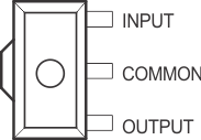
 Figure 5-3 PK Package,3-Pin SOT-89(Top View)
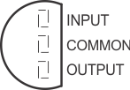
 Figure 5-2 LP Package,3-Pin TO-92(Top View)
| PIN | TYPE | DESCRIPTION | |||
|---|---|---|---|---|---|
| NAME | SOIC | TO-92 | SOT-89 | ||
| COMMON | 2, 3, 6, 7 | 2 | 2 | — | Ground |
| INPUT | 8 | 3 | 3 | I | Input pin. Use the recommended capacitor value as listed in the Recommended Operating Conditions table. Place the input capacitor as close to the IN and GND pins of the device as possible. |
| OUTPUT | 1 | 1 | 1 | O | Output pin. Use the recommended capacitor value as listed in the Recommended Operating Conditions table. Place the output capacitor as close to the OUT and GND pins of the device as possible. |
| NC | 4, 5 | — | — | — | No connect pin. This pin is not connected internally. Connect this pin to ground for best thermal performance or leave floating. |