JAJSP14F August 1995 – August 2022 UC1823A , UC1825A , UC2823A , UC2823B , UC2825A , UC2825B , UC3823A , UC3823B , UC3825A , UC3825B
PRODUCTION DATA
- 1特長
- 2概要
- 3Revision History
- 4Ordering Information
- 5Pin Configuration and Functions
- 6Specifications
- 7Application and Implementation
- 8Device and Documentation Support
- 9Mechanical, Packaging, and Orderable Information
パッケージ・オプション
デバイスごとのパッケージ図は、PDF版データシートをご参照ください。
メカニカル・データ(パッケージ|ピン)
- J|16
サーマルパッド・メカニカル・データ
発注情報
7.1 LEADING EDGE BLANKING
The UC3823A, UC2823B, UC3825A, and UC3825B perform fixed frequency pulse width modulation control. The UC3823A, and UC3823B outputs operate together at the switching frequency and can vary from zero to some value less than 100%. The UC3825A and UC3825B outputs are alternately controlled. During every other cycle, one output is off. Each output then switches at one-half the oscillator frequency, varying in duty cycle from 0 to less than 50%.
To limit maximum duty cycle, the internal clock pulse blanks both outputs low during the discharge time of the oscillator. On the falling edge of the clock, the appropriate output(s) is driven high. The end of the pulse is controlled by the PWM comparator, current limit comparator, or the overcurrent comparator.
Normally the PWM comparator senses a ramp crossing a control voltage (error amplifier output) and terminates the pulse. Leading edge blanking (LEB) causes the PWM comparator to be ignored for a fixed amount of time after the start of the pulse. This allows noise inherent with switched mode power conversion to be rejected. The PWM ramp input may not require any filtering as result of leading edge blanking.
To program a leading edge blanking (LEB) period, connect a capacitor, C, to CLK/LEB. The discharge time set by C and the internal 10-kΩ resistor determines the blanked interval. The 10-kΩ resistor has a 10% tolerance. For more accuracy, an external 2-kΩ 1% resistor (R) can be added, resulting in an equivalent resistance of 1.66 kΩ with a tolerance of 2.4%. The design equation is:
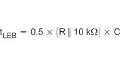
Values of R less than 2 kΩ should not be used.
Leading edge blanking is also applied to the current limit comparator. After LEB, if the ILIM pin exceeds the 1-V threshold, the pulse is terminated. The overcurrent comparator, however, is not blanked. It catches catastrophic overcurrent faults without a blanking delay. Any time the ILIM pin exceeds 1.2 V, the fault latch is set and the outputs driven low. For this reason, some noise filtering may be required on the ILIM pin.
 Figure 7-1 Leading Edge Blanking Operational Waveforms