JAJSH60A april   2019  – december 2020 UC1825B-SP

PRODUCTION DATA  

  1.   1
  2. 特長
  3. アプリケーション
  4. 概要
  5. Revision History
  6. Pin Configuration and Functions
  7. Specifications
    1. 6.1 Absolute Maximum Ratings
    2. 6.2 ESD Ratings
    3. 6.3 Recommended Operating Conditions
    4. 6.4 Thermal Information
    5. 6.5 Electrical Characteristics
    6. 6.6 Typical Characteristics
  8. Detailed Description
    1. 7.1 Overview
    2. 7.2 Functional Block Diagram
    3. 7.3 Feature Description
      1. 7.3.1 Control Methods
      2. 7.3.2 Synchronization
      3. 7.3.3 High Current Outputs
      4. 7.3.4 Open Loop Test Circuit
    4. 7.4 Device Functional Modes
  9. Application and Implementation
    1. 8.1 Application Information
    2. 8.2 Typical Application
      1. 8.2.1 System Design Theory
        1. 8.2.1.1 Switching Frequency
        2. 8.2.1.2 Transformer
        3. 8.2.1.3 RCD and Diode Clamp
        4. 8.2.1.4 Output Diode
        5. 8.2.1.5 Main Switching MOSFETs
        6. 8.2.1.6 Output Filter and Capacitance
        7. 8.2.1.7 Compensation
        8. 8.2.1.8 Sense Resistor
    3. 8.3 Application Curves
  10. Power Supply Recommendations
  11. 10Layout
    1. 10.1 Layout Guidelines
      1. 10.1.1 Feedback Traces
      2. 10.1.2 Input/Output Capacitors
      3. 10.1.3 Compensation Components
      4. 10.1.4 Traces and Ground Planes
      5. 10.1.5 Ground Planes
    2. 10.2 Layout Example
  12. 11Device and Documentation Support
    1. 11.1 Documentation Support
      1. 11.1.1 Related Documentation
    2. 11.2 ドキュメントの更新通知を受け取る方法
    3. 11.3 サポート・リソース
    4. 11.4 Trademarks
    5. 11.5 静電気放電に関する注意事項
    6. 11.6 用語集
  13. 12Mechanical, Packaging, and Orderable Information

パッケージ・オプション

メカニカル・データ(パッケージ|ピン)
サーマルパッド・メカニカル・データ
発注情報

Application Information

The oscillator of the UC1825B-SP is a saw tooth (see Figure 8-1). The rising edge is governed by a current controlled by the RT pin and value of capacitance at the CT pin (CCT). The falling edge of the sawtooth sets dead time for the outputs. Selection of RT must be done first, based on desired maximum duty cycle (see Figure 8-3). CT can then be chosen based on the desired frequency (RT) and DMAX (see Figure 8-2). Equation 1 shows the design equations.

Equation 1. GUID-F342281E-CE35-4230-8248-79CC596A66F2-low.gif

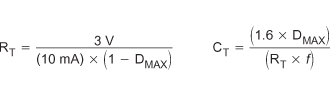
Recommended values for RT range from 1 kΩ to 100 kΩ. Control of DMAX less than 70% is not recommended.

GUID-E270E3BF-36FF-456D-B5F2-7E7729C9B60C-low.gifFigure 8-1 Oscillator
GUID-600F55A2-5227-4E0D-B4A3-132670256BED-low.gif
Figure 8-2 Oscillator Frequency vs Timing Resistance
GUID-C1FEB864-D847-485A-8475-978B87624239-low.gif
Figure 8-3 Maximum Duty Cycle vs Timing Resistance