JAJSH61A April   2019  – September 2019 UC1843B-SP

PRODUCTION DATA.  

  1. 特長
  2. アプリケーション
  3. 概要
    1.     Device Images
      1.      概略回路図
  4. 改訂履歴
  5. Pin Configuration and Functions
    1.     Pin Functions
  6. Specifications
    1. 6.1 Absolute Maximum Ratings
    2. 6.2 ESD Ratings
    3. 6.3 Recommended Operating Conditions
    4. 6.4 Thermal Information
    5. 6.5 Electrical Characteristics
    6. 6.6 Typical Characteristics
  7. Detailed Description
    1. 7.1 Overview
    2. 7.2 Functional Block Diagram
    3. 7.3 Feature Description
      1. 7.3.1 UVLO
      2. 7.3.2 Reference
      3. 7.3.3 Totem-Pole Output
    4. 7.4 Device Functional Modes
  8. Application and Implementation
    1. 8.1 Application Information
    2. 8.2 Typical Application
      1. 8.2.1 Design Requirements
      2. 8.2.2 Detailed Design Procedure
        1. 8.2.2.1 Switching Frequency
        2. 8.2.2.2 Transformer
        3. 8.2.2.3 RCD Diode Clamp
        4. 8.2.2.4 Output Diode
        5. 8.2.2.5 Output Filter and Capacitor
        6. 8.2.2.6 Compensation
        7. 8.2.2.7 Sense Resistor and Slope Compensation
      3. 8.2.3 Application Curves
  9. Power Supply Recommendations
  10. 10Layout
    1. 10.1 Layout Guidelines
      1. 10.1.1 Feedback Traces
      2. 10.1.2 Input/Output Capacitors
      3. 10.1.3 Compensation Components
      4. 10.1.4 Traces and Ground Planes
    2. 10.2 Layout Example
  11. 11デバイスおよびドキュメントのサポート
    1. 11.1 ドキュメントの更新通知を受け取る方法
    2. 11.2 コミュニティ・リソース
    3. 11.3 商標
    4. 11.4 静電気放電に関する注意事項
    5. 11.5 Glossary
  12. 12メカニカル、パッケージ、および注文情報

パッケージ・オプション

メカニカル・データ(パッケージ|ピン)
サーマルパッド・メカニカル・データ
発注情報

Power Supply Recommendations

The devices are designed to operate from an input voltage supply range between 8 V and 32 V. This input supply should be well regulated. If the input supply is located more than a few inches from the UC1843B-SP converter, additional bulk capacitance may be required in addition to the ceramic bypass capacitors. A tantalum capacitor with a value of 100 µF is a typical choice; however, this varies heavily on the start up circuitry of the device. This is because the input voltage to the device will decrease during start up and the input capacitance will have to provide enough charge to allow the UC1843B-SP to initially switch.
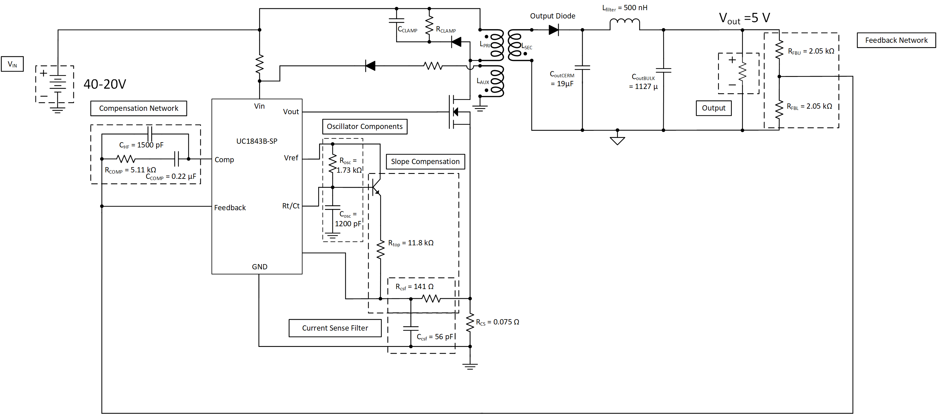
UC1843B-SP BlockDiagramDatasheet.pngFigure 15. Flyback Regulator