JAJSNI2A May   2008  – July 2022 UC2843A-Q1

PRODUCTION DATA  

  1. 特長
  2. アプリケーション
  3. 概要
  4. Revision History
  5. Pin Configuration and Functions
    1.     Pin Functions
  6. Specifications
    1. 6.1 Absolute Maximum Ratings
    2. 6.2 ESD Ratings
    3. 6.3 Recommended Operating Conditions
    4. 6.4 Electrical Characteristics
    5. 6.5 Thermal Information
    6. 6.6 Typical Characteristics
  7. Detailed Description
    1. 7.1 Overview
    2. 7.2 Functional Block Diagram
    3. 7.3 Feature Description
      1. 7.3.1 Pulse-by-Pulse Current Limiting
      2. 7.3.2 Current Sense Circuit
      3. 7.3.3 Error Amplifier Configuration
      4. 7.3.4 Undervoltage Lockout
      5. 7.3.5 Oscillator
    4. 7.4 Device Functional Modes
      1. 7.4.1 Normal Operation
      2. 7.4.2 Undervoltage Lockout (UVLO) Start-Up
      3. 7.4.3 UVLO Turnoff Mode
  8. Application and Implementation
    1. 8.1 Application Information
    2. 8.2 Typical Application
  9. Power Supply Recommendations
  10. 10Layout
    1. 10.1 Layout Guidelines
  11. 11Device and Documentation Support
    1. 11.1 Device Support
      1. 11.1.1 Development Support
        1. 11.1.1.1 Custom Design With WEBENCH® Tools
      2. 11.1.2 Device Nomenclature
    2. 11.2 Documentation Support
      1. 11.2.1 Related Documentation
    3. 11.3 Related Links
    4. 11.4 Receiving Notification of Documentation Updates
    5. 11.5 サポート・リソース
    6. 11.6 Trademarks
    7. 11.7 Electrostatic Discharge Caution
    8. 11.8 Glossary
  12. 12Mechanical, Packaging, and Orderable Information

パッケージ・オプション

メカニカル・データ(パッケージ|ピン)
サーマルパッド・メカニカル・データ
発注情報

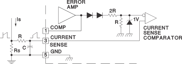
Current Sense Circuit

Peak current (IS) is determined by Equation 1:

Equation 1. GUID-AE6FA0F1-B7CD-4213-A396-D1B86D86C148-low.gif

A small RC filter may be required to suppress switch transients.
GUID-F26C2DC3-47DF-4085-9161-729AB5BA0C59-low.gifFigure 7-1 Current Sense Circuit Diagram