JAJSIW1A March 2020 – January 2024 UCC21739-Q1
PRODUCTION DATA
- 1
- 1 特長
- 2 アプリケーション
- 3 概要
- 4 Pin Configuration and Functions
-
5 Specifications
- 5.1 Absolute Maximum Ratings
- 5.2 ESD Ratings
- 5.3 Recommended Operating Conditions
- 5.4 Thermal Information
- 5.5 Power Ratings
- 5.6 Insulation Specifications
- 5.7 Safety-Related Certifications
- 5.8 Safety Limiting Values
- 5.9 Electrical Characteristics
- 5.10 Switching Characteristics
- 5.11 Insulation Characteristics Curves
- 5.12 Typical Characteristics
- 6 Parameter Measurement Information
-
7 Detailed Description
- 7.1 Overview
- 7.2 Functional Block Diagram
- 7.3
Feature Description
- 7.3.1 Power Supply
- 7.3.2 Driver Stage
- 7.3.3 VCC and VDD Undervoltage Lockout (UVLO)
- 7.3.4 Active Pulldown
- 7.3.5 Short Circuit Clamping
- 7.3.6 External Active Miller Clamp
- 7.3.7 Overcurrent and Short Circuit Protection
- 7.3.8 2-Level Turn-off
- 7.3.9 Fault ( FLT, Reset and Enable ( RST/EN)
- 7.3.10 Isolated Analog to PWM Signal Function
- 7.4 Device Functional Modes
-
8 Applications and Implementation
- 8.1 Application Information
- 8.2
Typical Application
- 8.2.1 Design Requirements
- 8.2.2
Detailed Design Procedure
- 8.2.2.1 Input filters for IN+, IN- and RST/EN
- 8.2.2.2 PWM Interlock of IN+ and IN-
- 8.2.2.3 FLT, RDY and RST/EN Pin Circuitry
- 8.2.2.4 RST/EN Pin Control
- 8.2.2.5 Turn-On and Turn-Off Gate Resistors
- 8.2.2.6 External Active Miller Clamp
- 8.2.2.7 Overcurrent and Short Circuit Protection
- 8.2.2.8 Isolated Analog Signal Sensing
- 8.2.2.9 Higher Output Current Using an External Current Buffer
- 8.2.3 Application Curves
- 9 Power Supply Recommendations
- 10Layout
- 11Device and Documentation Support
- 12Revision History
- 13Mechanical, Packaging, and Orderable Information
8.2.2.6 External Active Miller Clamp
External active miller clamp feature allows the gate driver to stay at the low status when the gate voltage is detected below VCLMPTH. When the other switch of the phase leg turns on, the dV/dt can cause a current through the parasitic miller capacitance of the switch and sink in the gate driver. The sinking current causes a negative voltage drop on the turn off gate resistance, and bumps up the gate voltage to cause a false turn on. The external active miller clamp features allows flexibility of board layout and active miller clamp pulldown strength. Limited by the board layout, if the driver cannot be placed close enough to the switch, external active miller clamp MOSFET can be placed close to the switch and the MOSFET can be chosen according to the peak current needed. Caution must be exercised when the driver is place far from the power semiconductor. Since the device has high peak sink and source current, the high dI/dt in the gate loop can cause a ground bounce on the board parasitics. The ground bounce can cause a positive voltage bump on CLMPE pin during the turn off transient, and results in the external active miller clamp MOSFET to turn on shortly and add extra drive strength to the sink current. To reduce the ground bounce, a 2Ω resistance is recommended to the gate of the external active clamp MOSFET.
When the VOUTH is detected to be lower than VCLMPTH above VEE, the CLMPE pin outputs a 5V voltage with respect to VEE, the external clamp FET is in linear region and the pulldown current is determined by the peak drain current, unless the on-resistance of the external clamp FET is large.
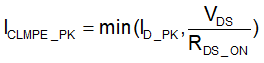
Where
- ID_PK is the peak drain current of the external clamp FET
- VDS is the drain-to-source voltage of the clamp FET when the CLMPE is activated
- RDS_ON is the on-resistance of the external clamp FET
The total delay time of the active miller clamp circuit from the gate voltage detection threshold VCLMPTH can be calculated as tDCLMPE+tCLMPER. tCLMPER depends on the parameter of the external active miller clamp MOSFET. As long as the total delay time is longer than the deadtime of high side and low side switches, the driver can effectively protect the switch from false turn on issue caused by miller effect.
 Figure 8-7 External Active Miller Clamp Configuration