JAJSHM6E june 2019 – february 2021 UCC256402 , UCC256403 , UCC256404
PRODUCTION DATA
- 1
- 1 特長
- 2 アプリケーション
- 3 概要
- 4 Revision History
- Device Comparison Table
- 5 Pin Configuration and Functions
- 6 Specifications
-
7 Detailed Description
- 7.1 Overview
- 7.2 Functional Block Diagram
- 7.3 Feature Description
- 7.4 Device Functional Modes
-
Application and Implementation
- 8.1 Application Information
- 8.2
Typical Application
- 8.2.1 Design Requirements
- 8.2.2
Detailed Design Procedure
- 8.2.2.1 LLC Power Stage Requirements
- 8.2.2.2 LLC Gain Range
- 8.2.2.3 Select Ln and Qe
- 8.2.2.4 Determine Equivalent Load Resistance
- 8.2.2.5 Determine Component Parameters for LLC Resonant Circuit
- 8.2.2.6 LLC Primary-Side Currents
- 8.2.2.7 LLC Secondary-Side Currents
- 8.2.2.8 LLC Transformer
- 8.2.2.9 LLC Resonant Inductor
- 8.2.2.10 LLC Resonant Capacitor
- 8.2.2.11 LLC Primary-Side MOSFETs
- 8.2.2.12 LLC Rectifier Diodes
- 8.2.2.13 LLC Output Capacitors
- 8.2.2.14 HV Pin Series Resistors
- 8.2.2.15 BLK Pin Voltage Divider
- 8.2.2.16 ISNS Pin Differentiator
- 8.2.2.17 VCR Pin Capacitor Divider
- 8.2.2.18 BW Pin Voltage Divider
- 8.2.2.19 Soft Start and Burst Mode Programming
- 8.2.3 Application Curves
- 8 Power Supply Recommendations
- 9 Layout
- 10Device and Documentation Support
- Mechanical, Packaging, and Orderable Information
7.3.6 Bulk Voltage Sensing
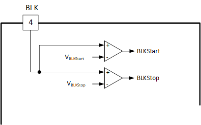
The BLK pin is used to sense the LLC DC input voltage (bulk voltage) level. The comparators on BLK pin have the following two thresholds:
- Bulk voltage level when LLC starts switching – VBLKStart
- Bulk voltage level when LLC stops switching – VBLKStop
A resistor divider is connected to the pin to achieve the desired system input range. A fault is triggered if BLK pin voltage drops lower than VBLKStop during operation. The detailed action of Input Under Voltage Protection is described in Section 7.3.9.4 section.
Figure 7-8 shows the block diagram of the BLK pin.
 Figure 7-8 BLK Pin Block Diagram
BLK voltage is also used to monitor the input over voltage fault for some device versions as listed in Section 5. There are two thresholds:
- Bulk voltage level when BLK over voltage protection (OVP) rising threshold - VBLKOVPRise
- Bulk voltage level when BLK over voltage protection (OVP) falling threshold - VBLKOVPFall
When BLK voltage is higher than VBLKOVPRise, OVP is triggered; OVP gets cleared when BLK voltage falls below VBLKOVPFall.