JAJSHM6E june   2019  – february 2021 UCC256402 , UCC256403 , UCC256404

PRODUCTION DATA  

  1.   1
  2. 特長
  3. アプリケーション
  4. 概要
  5. Revision History
  6.   Device Comparison Table
  7. Pin Configuration and Functions
    1.     Pin Functions
  8. Specifications
    1. 6.1 Absolute Maximum Ratings
    2. 6.2 ESD Ratings
    3. 6.3 Recommended Operating Conditions
    4. 6.4 Thermal Information
    5. 6.5 Electrical Characteristics
    6. 6.6 Switching Characteristics
    7. 6.7 Typical Characteristics
  9. Detailed Description
    1. 7.1 Overview
    2. 7.2 Functional Block Diagram
    3. 7.3 Feature Description
      1. 7.3.1 Hybrid Hysteretic Control
      2. 7.3.2 Regulated 13-V Supply
      3. 7.3.3 Feedback Chain
        1. 7.3.3.1 Optocoupler Feedback Signal Input and Bias
        2. 7.3.3.2 FB Pin Voltage Clamp
        3. 7.3.3.3 "Pick Lower Value" Block and Soft Start Multiplexer
        4. 7.3.3.4 Pick Higher Block and Burst Mode Multiplexer
        5. 7.3.3.5 VCR Comparators
      4. 7.3.4 Resonant Capacitor Voltage Sensing
      5. 7.3.5 Resonant Current Sensing
      6. 7.3.6 Bulk Voltage Sensing
      7. 7.3.7 Output Voltage Sensing
      8. 7.3.8 High Voltage Gate Driver
        1. 7.3.8.1 Adaptive Dead Time Control
      9. 7.3.9 Protections
        1. 7.3.9.1 ZCS Region Prevention
        2. 7.3.9.2 Over Current Protection (OCP)
        3. 7.3.9.3 Bias Winding Over Voltage Protection (BWOVP)
        4. 7.3.9.4 Input Under Voltage Protection (VINUVP)
        5. 7.3.9.5 Input Over Voltage Protection (VINOVP)
        6. 7.3.9.6 Boot UVLO
        7. 7.3.9.7 RVCC UVLO
        8. 7.3.9.8 Over Temperature Protection (OTP)
    4. 7.4 Device Functional Modes
      1. 7.4.1 High Voltage Start-Up
      2. 7.4.2 X-Capacitor Discharge
      3. 7.4.3 Burst Mode Control
        1. 7.4.3.1 Soft-Start and Burst-Mode Threshold
        2. 7.4.3.2 BMTL/BMTH Ratio Programming
      4. 7.4.4 System State Machine
  10.   Application and Implementation
    1. 8.1 Application Information
    2. 8.2 Typical Application
      1. 8.2.1 Design Requirements
      2. 8.2.2 Detailed Design Procedure
        1. 8.2.2.1  LLC Power Stage Requirements
        2. 8.2.2.2  LLC Gain Range
        3. 8.2.2.3  Select Ln and Qe
        4. 8.2.2.4  Determine Equivalent Load Resistance
        5. 8.2.2.5  Determine Component Parameters for LLC Resonant Circuit
        6. 8.2.2.6  LLC Primary-Side Currents
        7. 8.2.2.7  LLC Secondary-Side Currents
        8. 8.2.2.8  LLC Transformer
        9. 8.2.2.9  LLC Resonant Inductor
        10. 8.2.2.10 LLC Resonant Capacitor
        11. 8.2.2.11 LLC Primary-Side MOSFETs
        12. 8.2.2.12 LLC Rectifier Diodes
        13. 8.2.2.13 LLC Output Capacitors
        14. 8.2.2.14 HV Pin Series Resistors
        15. 8.2.2.15 BLK Pin Voltage Divider
        16. 8.2.2.16 ISNS Pin Differentiator
        17. 8.2.2.17 VCR Pin Capacitor Divider
        18. 8.2.2.18 BW Pin Voltage Divider
        19. 8.2.2.19 Soft Start and Burst Mode Programming
      3. 8.2.3 Application Curves
  11. Power Supply Recommendations
    1. 8.1 VCC Pin Capacitor
    2. 8.2 Boot Capacitor
    3. 8.3 RVCC Pin Capacitor
  12. Layout
    1. 9.1 Layout Guidelines
    2. 9.2 Layout Example
  13. 10Device and Documentation Support
    1. 10.1 Documentation Support
      1. 10.1.1 Related Documentation
    2. 10.2 Related Links
    3. 10.3 Receiving Notification of Documentation Updates
    4. 10.4 Community Resources
    5. 10.5 Trademarks
  14.   Mechanical, Packaging, and Orderable Information

パッケージ・オプション

メカニカル・データ(パッケージ|ピン)
サーマルパッド・メカニカル・データ
発注情報

BW Pin Voltage Divider

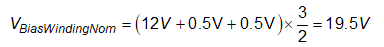
The BW pin programs the ratio between burst mode entry and exit thresholds as well as senses the output voltage through the bias winding and protects the power stage from over voltage. The nominal output voltage is 12 V. The bias winding has 3 turns, and the secondary side winding has 2 turns. Assuming there is a 0.5-V drop in the rectifier diodes (Vf) and a further 0.5-V drop due to other losses (Vloss), the nominal voltage of the bias winding is given by:

Equation 63. GUID-0572612B-AAC8-43F0-B10A-12373B14E6B1-low.gif

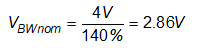
The desired OVP threshold in this design is 140% of the nominal value. The OVP threshold level in UCC25640x device is 4 V, so the nominal BW pin voltage is given by:

Equation 64. GUID-14400088-2664-4EF1-BC91-A656DE494119-low.gif

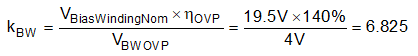
The required BW divider ratio is then given by:

Equation 65. GUID-B1E65D91-6587-44E1-B2A5-7DA919817A1C-low.gif

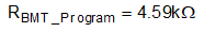
In this design, the burst mode threshold ratio is chosen to be 0.6 (Option 6).The target programming resistance is then:

Equation 66. GUID-6A855ACB-9E91-47F9-9037-7FBCD06A515F-low.gif

The lower BW resistor can be calculated by:

Equation 67. GUID-A9EEE2D1-2551-4EF5-BB43-EDFEA1134201-low.gif

A standard value of 5.36 kΩ is chosen for the lower BW resistor.

The upper resistor can be calculated by:

Equation 68. GUID-A9CD1187-70BE-441D-827B-4C905450F1E0-low.gif

A standard value of 30.9 kΩ is chosen for the upper BW resistor.