JAJSNN2A October 2023 – December 2023 UCC25660
PRODUCTION DATA
- 1
- 1 特長
- 2 アプリケーション
- 3 概要
- 4 Device Comparison Table
- 5 Pin Configuration and Functions
- 6 Specifications
-
7 Detailed Description
- 7.1 Overview
- 7.2 Functional Block Diagram
- 7.3 Feature Description
- 7.4 Protections
- 7.5 Device Functional Modes
-
8 Application and Implementation
- 8.1 Application Information
- 8.2
Typical Application
- 8.2.1 Design Requirements
- 8.2.2
Detailed Design Procedure
- 8.2.2.1 LLC Power Stage Requirements
- 8.2.2.2 LLC Gain Range
- 8.2.2.3 Select Ln and Qe
- 8.2.2.4 Determine Equivalent Load Resistance
- 8.2.2.5 Determine Component Parameters for LLC Resonant Circuit
- 8.2.2.6 LLC Primary-Side Currents
- 8.2.2.7 LLC Secondary-Side Currents
- 8.2.2.8 LLC Transformer
- 8.2.2.9 LLC Resonant Inductor
- 8.2.2.10 LLC Resonant Capacitor
- 8.2.2.11 LLC Primary-Side MOSFETs
- 8.2.2.12 Design Considerations for Adaptive Dead-Time
- 8.2.2.13 LLC Rectifier Diodes
- 8.2.2.14 LLC Output Capacitors
- 8.2.2.15 HV Pin Series Resistors
- 8.2.2.16 BLK Pin Voltage Divider
- 8.2.2.17 ISNS Pin Differentiator
- 8.2.2.18 TSET Pin
- 8.2.2.19 OVP/OTP Pin
- 8.2.2.20 Burst Mode Programming
- 8.2.2.21 Application Curves
- 8.3 Power Supply Recommendations
- 8.4 Layout
- 9 Revision History
- 10Mechanical, Packaging, and Orderable Information
7.3.2 VCR Synthesizer
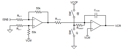
The UCC25660 implements a VCR Synthesizer which integrates the resonant tank current to form a internal representation of the resonant capacitor voltage. By implementing the VCR synthesizer internally, the UCC25660 provides for an ability to support very high frequency startup with controlled inrush currents and feed forward gain stage. The internal VCR synthesizer also makes the controller less succeptible to external noise picked up on the ISNS pin, making the controller more robust.
 Figure 7-3 VCR Synthesizer Block
Diagram
Figure 7-3 VCR Synthesizer Block
DiagramThe first stage of the VCR synthesizer consists of a programable gain stage, used to implement the input voltage feed forward function. The second stage consist of a programable integrator with ramp compensation.
To accommodate a wide frequency range of LLC power stages, the time constant of the integrator is externally configurable at startup to meet the needs of the design using the TSET pin. A voltage resistor divider between V5P and GNDP, connecting to TSET pin, configures the TSET settings. The UCC25660 detected the divider ratio during startup. Based on the divider ratio, not only the time constant but the OCP threshold can be choosen. Once the time constant is chosen, the maximum dead-time is also configured. The column 2 in the tabled indicates the minimum frequency upto which the IPPC operation is maintained. Once the frequency falls below this, the controller can still maintian closed loop operation and works as a conventional current mode control.
|
TSET Option # |
TSET Voltage (V) for 3.5V OCP |
TSET Voltage (V) for 4V OCP |
Minimum Frequency for IPPC Operation (kHz) |
Integrator Time Constant (ns) |
Maximum dead-time (μs) |
|---|---|---|---|---|---|
| 17 | 2.295 | 2.686 | 698.6 | 68 | 0.5 |
| 16 | 2.168 | 2.813 | 591.6 | 80 | 0.5 |
| 15 | 2.041 | 2.941 | 501 | 93 | 0.5 |
| 14 | 1.914 | 3.068 | 424.3 | 112 | 0.5 |
| 13 | 1.787 | 3.196 | 359.3 | 132 | 1 |
| 12 | 1.66 | 3.323 | 304.3 | 156 | 1 |
| 11 | 1.533 | 3.441 | 256.7 | 184 | 1 |
| 10 | 1.416 | 3.568 | 218.2 | 214 | 1 |
| 9 | 1.299 | 3.696 | 184.8 | 257 | 1 |
| 8 | 1.182 | 3.813 | 156.5 | 304 | 1 |
| 7 | 1.074 | 3.921 | 132.5 | 359 | 1 |
| 6 | 0.967 | 4.029 | 112.2 | 424 | 1 |
| 5 | 0.850 | 4.147 | 95 | 490 | 1 |
| 4 | 0.742 | 4.254 | 80.5 | 588 | 1 |
| 3 | 0.644 | 4.352 | 68.1 | 694 | 1 |
| 2 | 0.547 | 4.450 | 57.7 | 820 | 1 |
| 1 | 0.450 | 4.549 | 48.9 | 968 | 1 |
| X | <0.392 | >4.607 | X | X | X |