JAJSLJ6C november 2020 – august 2023 UCC25800-Q1
PRODUCTION DATA
- 1
- 1 特長
- 2 アプリケーション
- 3 概要
- 4 Revision History
- 5 Device Comparison Table
- 6 Pin Configuration and Functions
- 7 Specifications
- 8 Detailed Description
- 9 Application and Implementation
- 10Power Supply Recommendations
- 11Layout
- 12Device and Documentation Support
- 13Mechanical, Packaging, and Orderable Information
パッケージ・オプション
メカニカル・データ(パッケージ|ピン)
- DGN|8
サーマルパッド・メカニカル・データ
- DGN|8
発注情報
9.2.3 Detailed Design Procedure
The design of the isolated bias supply based on the UCC25800-Q1 transformer driver involves both the power-stage design and the controller parameters design.
The power-stage design involves the selection of the transformer and the resonant capacitors. Traditionally, the LLC transformer design is complicated because the design goal is to optimize the efficiency performance, the input and output voltage ranges, achieving ZVS, as well as minimizing the size of the transformer. It is a lot easier when design the transformer for the isolated bias supply because the design goal is to make it simple and robust. The efficiency is important but not critical since the gate driver power is a tiny portion of the overall system power.
Step 1: Transformer turns-ratio selection
Because this isolated bias supply operates with open-loop control, the voltage accuracy is not able to get down to 1%. The post regulators, such as a linear regulator can be used to achieve 1% regulation accuracy. Therefore, when designing the LLC converter output voltage, the headroom for the post regulator stage needs to be considered.
At the resonant frequency, together with the voltage doubler output, the LLC converter voltage gain is equal to the transformer turns-ratio. Therefore, the transformer turns-ratio can be calculated as:
Where:
- VF is the output diode forward voltage drop
- Vheadroom is the extra headroom needed for the post regulator
Step 2: Calculate transformer volt-second rating
The transformer volt-second rating on the primary side can be calculated as:
Step 3: Calculate the transformer currents
The transformer sees highest RMS current right before over current protection. According to Figure 9-6, the output current is equal to the average current of the secondary-side rectified current. When load current is at the over current protection level of 100 mA, the primary side current can be calculated. The transformer primary-side and secondary-side peak and RMS current can be calculated based on Equation 12 through Equation 15.
From step 1 through 3, the key transformer information can be summarized in Table 9-2. It can be used to share with transformer vender to get the transformer designed and manufactured. It is recommended to leave some design margins (30%~50%) for the current ratings to consider the tolerance of the components.
| Parameter Name | Value | Unit |
|---|---|---|
| Primary side to secondary side turns ratio | 0.6 | |
| Primary side volt-second | 3.75 | Vμs |
| Primary side peak current | 523 | mA |
| Primary side RMS current | 370 | mA |
| Secondary side peak current | 314 | mA |
| Secondary side RMS current | 222 | mA |
To minimize the transformer inter-winding capacitance, the split chamber bobbin is recommended, as shown in Figure 9-7.
 Figure 9-7 Split chamber bobbin
Another key transformer parameter is the magnetizing inductance. In traditional LLC converter design, the magnetizing inductor is used to achieve ZVS and the desired voltage gain to cover the entire input and output voltage range. Given the open-loop LLC operates with fixed input and output voltages, the sole goal of the magnetizing inductor is to achieve ZVS. Based on the ZVS criteria, the design target of the magnetizing inductance can be calculated based on Equation 16. In this equation, Lm is the magnetizing inductor value, td is the dead-time, fSW is the switching frequency, and CSW is the SW-pin parasitic capacitance (it has a typical value of 170 pF). With 500-kHz switching frequency and 50-ns of dead-time, the magnetizing inductance can be calculated as 73.5 μH. This inductor value gives an initial design target of the transformer and the final value can be different. If the magnetizing inductance is larger, it does not have enough magnetizing current to achieve full ZVS. With the low input voltage and small parasitic capacitance on the switch node, partial ZVS still brings in the EMI and loss reduction benefit. If the magnetizing inductance is smaller than the target, it'll create more current than needed, which results in extra conduction loss. But the loss increase is limited without causing concerns on the thermal stress or efficiency. Normally, it is recommended to use the core without an air gap, and the transformer magnetizing inductance is more than 20 times higher than the leakage inductance Otherwise, a minimum air gap is recommended without causing extra manufacture cost.
Step 4: Select resonant capacitor
The resonant capacitor selection is based on the resonant frequency. Choose the resonant tank resonant frequency 10~15% above the switching frequency.
When using the voltage double rectifier, each resonant capacitor value should be half of this value. Therefore, a 22-nF resonant capacitor can be used on each of the resonant capacitor.
Step 5: Choose output capacitor
The output capacitor selection is based on the output voltage ripple requirement. The output capacitor can be calculated based on Equation 18. Design the capacitor based on half of the ripple amplitude so that there is margin for the voltage ripple caused by the capacitor ESR. Choose the output capacitor needs to consider both the ripple requirement and the gate driver requirement. A 10-μF capacitor can be used in this case. It should be noticed that the ceramic capacitor loses its capacitance when the voltage is applied.
Step 6: Choose primary side DC blocking capacitor
The primary-side half-bridge DC blocking capacitors need to be much larger than the resonant capacitor. Given the high-switching frequency design, low ESR X7R capacitors with value between 1 μF and 10 μF are recommended.
Once the power stage is set up, the programming pins of the IC can be set up accordingly. Given the minimum external components, setting up the UCC25800-Q1 is extremely easy.
Step 7: Setting up RT pin resistor
To set the switching frequency to 500 kHz, according to the description in Oscillator, the RT pin resistor can be calculated as:
Given 50 kΩ is not a standard resistor value, choose an RRT value of 49.9 kΩ.
Step 8: Setting up OC/DT pin resistor divider
The OC/DT pin is a multi-function pin. It sets the maximum dead-time for the adaptive dead-time, and sets the OCP levels for over current protection.
For the dead-time setting, generally choose 5 % to 10% of the switching cycle, as the maximum dead-time. This value can be further adjusted according to the measurement result, depending on the soft switching conditions. Equation 3 calculates the voltage on DT/CT pin:
The OCP setting is determined by the primary-side peak current. In Equation 15, the primary-side peak current is calculated as 523 mA. Leaving extra 30% margin, the OCP1 level should be roughly 680 mA. OCP1_4 can be used as the OCP1 setting.
According to Table 8-1, the Thevenin resistance should be between 7.95 kΩ and 8.25 kΩ. We can use the value in the middle to set up the resistor and verify the Thevenin resistance after the resistor values are calculated,
The pull-up resistor can be calculated as
And the pull-down resistor can be calculated as
It can be seen, due to the limited standard resistor value, the selected resistor values are different than the calculated resistor values. The Thevenin resistance needs to be checked. In this case, the Thevenin resistance is 8.058 kΩ and it is within the OCP1_4 setting range.
The UCC25800-Q1 based LLC converter can output a single output. It needs some help to split it into the dual outputs needed for the final designs. Depending on the regulation accuracy requirement, the splitting can be done using a simple Zener diode, a shunt-regulator, or even with a linear regulator, as demonstrated in Figure 9-8.
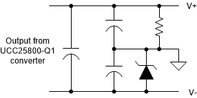 |
| (a) Split the output voltage using Zener diode |
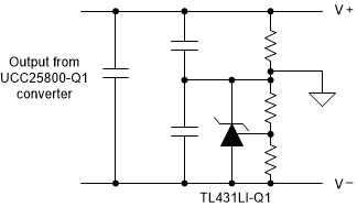 |
| (b) Split the output voltage using shunt-regulator |
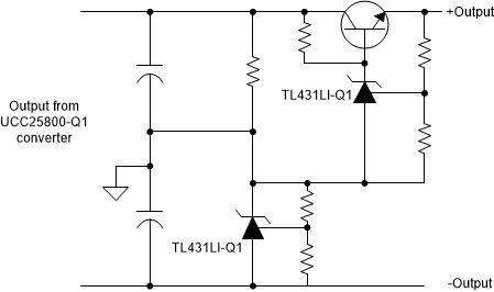 |
| (c) splitting the output voltage using shunt-regulator and linear regulator |
Using the Zener diode, the negative rail voltage is determined by the Zener voltage and the rest of the output voltage becomes the positive rail. Due to the tolerance of the Zener diode, a shunt-regulator can be used to improve the negative rail voltage accuracy. Furthermore, a linear regulator can be added to improve the positive rail voltage accuracy as well. The designer can choose the right solution based on the performance and cost tradeoffs.
In this design, the shunt-regulator and linear-regulator are used to get 1% accuracy required for the positive and negative rail. ATL431-Q1 is used as the shunt-regulator and the voltage reference for the linear regulator. Given the reference voltage of ATL431-Q1 is 2.5 V, to create 5-V shunt-regulator voltage, a 1-kΩ and 1-kΩ voltage divider can be used to set up the 5-V regulation voltage. On the positive rail side, to create 18-V output voltage, 6.34 kΩ and 1 kΩ can be used to set up the output voltage divider ((6.34+1)✕2.5V=18.35V).
With all the calculated circuit parameters, the design schematic is shown in Figure 9-9.
 Figure 9-9 Circuit schematic for the designed
isolated bias supply
Figure 9-9 Circuit schematic for the designed
isolated bias supply