JAJSC44B August 2015 – March 2017 UCC27714
PRODUCTION DATA.
- 1 特長
- 2 アプリケーション
- 3 概要
- 4 改訂履歴
- 5 Pin Configuration and Functions
- 6 Specifications
- 7 Detailed Description
-
8 Application and Implementation
- 8.1 Application Information
- 8.2
Typical Application
- 8.2.1 Design Requirements
- 8.2.2
Detailed Design Procedure
- 8.2.2.1 Selecting HI and LI Low Pass Filter Components (RHI, RLI, CHI, CLI)
- 8.2.2.2 Selecting Bootstrap Capacitor (CBOOT)
- 8.2.2.3 Selecting VDD Bypass/Holdup Capacitor (CVDD) and Rbias
- 8.2.2.4 Selecting Bootstrap Resistor (RBOOT)
- 8.2.2.5 Selecting Gate Resistor RHO/RLO
- 8.2.2.6 Selecting Bootstrap Diode
- 8.2.2.7 Estimate the UCC27714 Power Losses (PUCC27714)
- 8.2.2.8 Application Example Schematic Note
- 8.2.2.9 LO and HO Overshoot and Undershoot
- 8.2.3 Application Curves
- 9 Power Supply Recommendations
- 10Layout
- 11デバイスおよびドキュメントのサポート
- 12メカニカル、パッケージ、および注文情報
6 Specifications
6.1 Absolute Maximum Ratings(1) (2)
Over operating free-air temperature range (unless otherwise noted), all voltages are with respect to COM (unless otherwise noted), currents are positive into and negative out of the specified terminal. (1)| MIN | MAX | UNIT | |||
|---|---|---|---|---|---|
| VIN | Input voltage range | HI, LI, EN(3) with respect to VSS | –5 | 20 | V |
| VDD supply voltage | –0.3 | 20 | V | ||
| HB | –0.3 | 640 | V | ||
| HB-HS | –0.3 | 20 | V | ||
| VOUT | Output voltage range, HO | DC | HS – 0.3 | HB + 0.3 | V |
| Transient, less than 100 ns(4) | HS – 2 | HB + 0.3 | V | ||
| Output voltage range, LO | DC | –0.3 | VDD + 0.3 | V | |
| Transient, less than 100 ns(4) | –2 | VDD + 0.3 | V | ||
| Logic ground, With respect to COM | –7 | 6 | V | ||
| Logic ground, VDD-VSS | –0.3 | 20 | V | ||
| IOUT | Output current, HO, LO, IOUT_PULSED (100 ns) | ±4 | A | ||
| IOUT | Output current, HO, LO, IOUT_DC | 0.25 | A | ||
| dVHS/dt | Allowable offset supply voltage transient | –50 | 50 | V/ns | |
| Lead temperature (soldering, 10 second) | 300 | °C | |||
| TJ | Junction temperature range | –40 | 150 | °C | |
| Tstg | Storage temperature range | -65 | 150 | °C | |
(1) Stresses beyond those listed under Absolute Maximum Ratings may cause permanent damage to the device. These are stress ratings only, which do not imply functional operation of the device at these or any other conditions beyond those indicated under Recommended Operating Conditions. Exposure to absolute-maximum-rated conditions for extended periods may affect device reliability.
(2) See Packaging Section of the datasheet for thermal limitations and considerations of packages.
(3) The maximum voltage on the Input pins is not restricted by the voltage on the VDD pin.
(4) Values are verified by characterization on bench.
6.2 ESD Ratings
| VALUE | UNIT | ||||
|---|---|---|---|---|---|
| V(ESD)(1) | Electrostatic discharge | Human body model, HBM | ±1400 | V | |
| Charge device model, CDM | ±500 | V | |||
(1) These devices are sensitive to electrostatic discharge; follow proper device handing procedures
6.3 Recommended Operating Conditions
All voltages are with respect to COM, –40°C < TJ < 125°C, currents are positive into, negative out of the specified terminals| MIN | NOM | MAX | UNIT | ||
|---|---|---|---|---|---|
| VDD | Supply voltage | 10 | 17 | V | |
| HB-HS | Driver bootstrap voltage | 10 | 17 | V | |
| HS | Source terminal voltage(1) | –8 | 600 | V | |
| HB | Bootstrap pin voltage | HS + 10 | HS + 17 | V | |
| HI, LI, EN | Input voltage with respect to VSS | –4 | 17 | V | |
| VSS | Logic ground | –6(2) | 5(3) | V | |
| TJ | Junction temperature | –40 | 125 | °C | |
(1) Logic operational for HS of –8 V to 600 V at HB – HS = 12 V
(2) At VDD – COM = 10 V
(3) At VDD – COM = 15 V
6.4 Thermal Information
| THERMAL METRIC(1) | UCC27714 | UNIT | |
|---|---|---|---|
| D (SOIC) | |||
| PINS | |||
| RθJA | Junction-to-ambient thermal resistance | 72.3 | °C/W |
| RθJC(top) | Junction-to-case (top) thermal resistance | 31.8 | °C/W |
| RθJB | Junction-to-board thermal resistance | 26.5 | °C/W |
| ψJT | Junction-to-top characterization parameter | 3.6 | °C/W |
| ψJB | Junction-to-board characterization parameter | 26.2 | °C/W |
| RθJC(bot) | Junction-to-case (bottom) thermal resistance | N/A | °C/W |
(1) For more information about traditional and new thermal metrics, see the IC Package Thermal Metrics application report, SPRA953.
6.5 Electrical Characteristics
At VDD = VHB = 15 V, VSS = VHS = 0, all voltages are with respect to COM, no load on LO and HO, –40°C < TJ < 125°C, current are positive into and negative out of the specified terminal, over operating free-air temperature range (unless otherwise noted)| PARAMETER | TEST CONDITIONS | MIN | TYP | MAX | UNIT | |
|---|---|---|---|---|---|---|
| SUPPLY BLOCK | ||||||
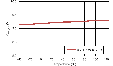
| VVDD(on) | turn-on threshold voltage of VDD | 8.4 | 9.1 | 9.8 | V | |
| VVDD(off) | turn-off threshold voltage of VDD | 7.9 | 8.6 | 9.3 | V | |
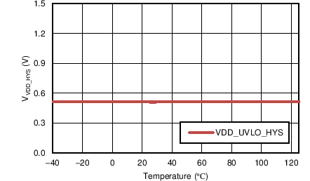
| VVDD(hys) | Hysteresis of VDD | 0.4 | 0.5 | - | V | |
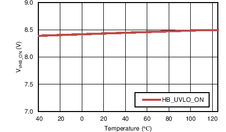
| VVHB(on) | turn-on threshold voltage of VHB-VHS | 7.7 | 8.3 | 9.0 | V | |
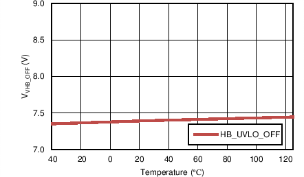
| VVHB(off) | turn-off threshold voltage of VHB-VHS | 6.7 | 7.25 | 8.05 | V | |
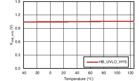
| VVHB(hys) | Hysteresis of VHB-VHS | 0.5 | 1.0 | - | V | |
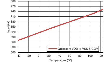
| IQDD | Total quiescent VDD to VSS and COM supply current | HI = LI = 0 V or 5 V, DC on/off state | 750 | 1050 | µA | |
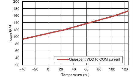
| IQCOM | Quiescent VDD-COM supply current | HI = LI = 0 V or 5 V, DC on/off state | 175 | 350 | µA | |
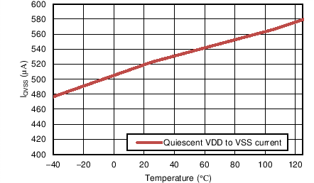
| IQVSS | Quiescent VDD-VSS supply current | HI = LI = 0 V or 5 V, DC on/off state | 550 | 750 | µA | |
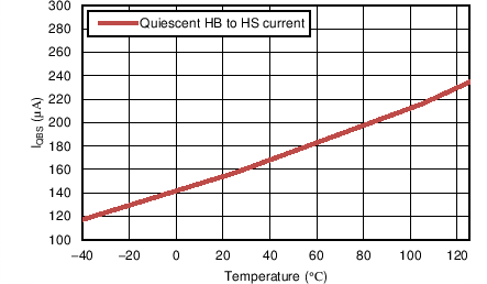
| IQBS | Quiescent HB-HS supply current | HI = 0 V or 5 V, HO in DC on/off state | 120 | 300 | µA | |
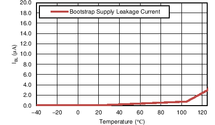
| IBL | Bootstrap Supply Leakage Current | HB = HS = 600 V | 20 | µA | ||
| INPUT AND ENABLE BLOCK | ||||||
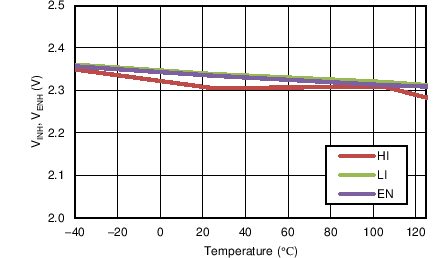
| VINH, VENH | Input pin (HI or LI) and enable pin (EN) High threshold | 1.7 | 2.3 | 2.7 | V | |
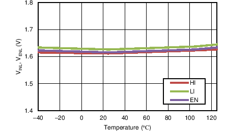
| VINL, VENL | Input pin (HI or LI) and enable pin (EN) low threshold | 1.2 | 1.6 | 2.1 | V | |
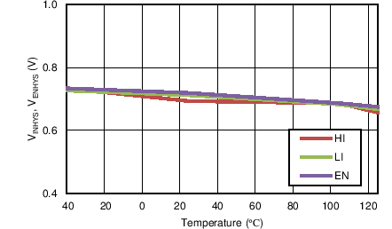
| VINHYS, VENHYS | Input pin (HI or LI) and enable pin (EN) threshold hysteresis | 0.7 | V | |||
| IINL | HI, LI input low bias current | HI, LI = 0 V | -5 | 0 | 5 | µA |
| IINH | HI, LI input high bias current | HI, LI = 5 V | 3 | 65 | µA | |
| IENL | EN input low bias current | VEN = 0 V | -90 | -50 | µA | |
| IENH | EN input high bias current | VEN = 5 V | -65 | -25 | µA | |
| RHI | Pull-down resistor on HI input pin | 400 | kΩ | |||
| RLI | Pull-down resistor on LI input pin | 400 | kΩ | |||
| REN | Pull-up resistor on enable pin | 200 | kΩ | |||
| OUTPUT BLOCK | ||||||
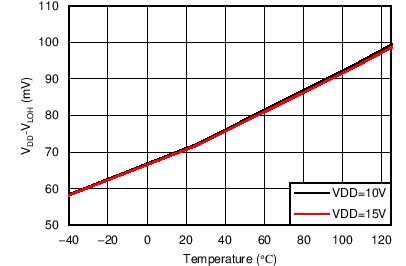
| VDD-VLOH | LO output high voltage | LI = 5 V, ILO = –20 mA | 70 | 120 | mV | |
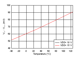
| VHB-VHOH | HO output high voltage | HI = 5 V, IHO = –20 mA | 70 | 120 | mV | |
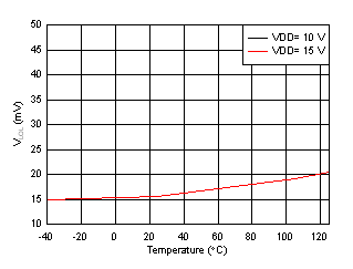
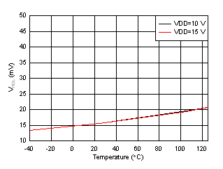
| VLOL | LO output low voltage | LI = 0 V, ILO = 20 mA | 15 | 35 | mV | |
| VHOL | HO output low voltage | HI = 0 V, IHO = 20 mA | 20 | 40 | mV | |
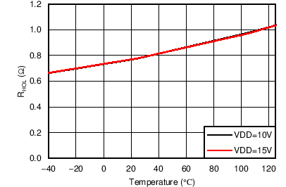
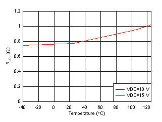
| RLOL, RHOL (2) | LO, HO output pull down resistance | ILO = 20 mA, IHO = 20 mA | 1.45 | Ω | ||
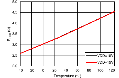
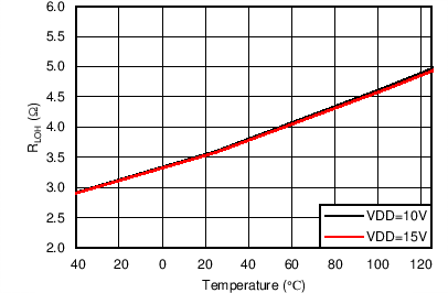
| RLOH, RHOH | LO, HO output pull up resistance | ILO = –20 mA, IHO= –20 mA | 3.75 | 5.8 | Ω | |
| IGPK- (1) | HO. LO output low short circuit pulsed current | HI = L = 0 V, HO = LO = 15 V, PW < 10 µs | 4 | A | ||
| IGPK+ (1) | HO. LO output high short circuit pulsed current | H I= LI = 5 V, HO = LO = 0 V, PW < 10 µs | 4 | A | ||
(1) Ensured by Design, Not tested in production
(2) ROH represents on-resistance of only the P-Channel MOSFET device in pull-up structure of UCC27714 output stage. Refer to Output Stage
6.6 Timing Requirements
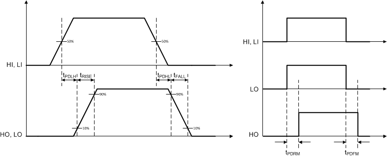 Figure 1. Typical Test Timing Diagram
6.7 Typical Characteristics
