SLUSBL5A February 2015 – June 2019 UCC28730
PRODUCTION DATA.
- 1 Features
- 2 Applications
- 3 Description
- 4 Revision History
- 5 Pin Configuration and Functions
- 6 Specifications
-
7 Detailed Description
- 7.1 Overview
- 7.2 Functional Block Diagram
- 7.3 Feature Description
- 7.4 Device Functional Modes
-
8 Application and Implementation
- 8.1 Application Information
- 8.2
Typical Application
- 8.2.1 Design Requirements
- 8.2.2
Detailed Design Procedure
- 8.2.2.1 Stand-By Power Estimate
- 8.2.2.2 Input Bulk Capacitance and Minimum Bulk Voltage
- 8.2.2.3 Transformer Turns Ratio, Inductance, Primary-Peak Current
- 8.2.2.4 Transformer Parameter Verification
- 8.2.2.5 Output Capacitance
- 8.2.2.6 VDD Capacitance, CVDD
- 8.2.2.7 VS Resistor Divider, Line Compensation, and Cable Compensation
- 8.2.2.8 VS Wake-Up Detection
- 8.2.3 Application Curves
- 8.3 Do's and Don'ts
- 9 Power Supply Recommendations
- 10Layout
-
11Device and Documentation Support
- 11.1
Device Support
- 11.1.1 Development Support
- 11.1.2
Device Nomenclature
- 11.1.2.1 Capacitance Terms in Farads
- 11.1.2.2 Duty-Cycle Terms
- 11.1.2.3 Frequency Terms in Hertz
- 11.1.2.4 Current Terms in Amperes
- 11.1.2.5 Current and Voltage Scaling Terms
- 11.1.2.6 Transformer Terms
- 11.1.2.7 Power Terms in Watts
- 11.1.2.8 Resistance Terms in Ω
- 11.1.2.9 Timing Terms in Seconds
- 11.1.2.10 DC Voltage Terms in Volts
- 11.1.2.11 AC Voltage Terms in Volts
- 11.1.2.12 Efficiency Terms
- 11.2 Documentation Support
- 11.3 Receiving Notification of Documentation Updates
- 11.4 Community Resources
- 11.5 Trademarks
- 11.6 Electrostatic Discharge Caution
- 11.7 Glossary
- 11.1
Device Support
- 12Mechanical, Packaging, and Orderable Information
7.3.5 Wake-Up Detection and Function
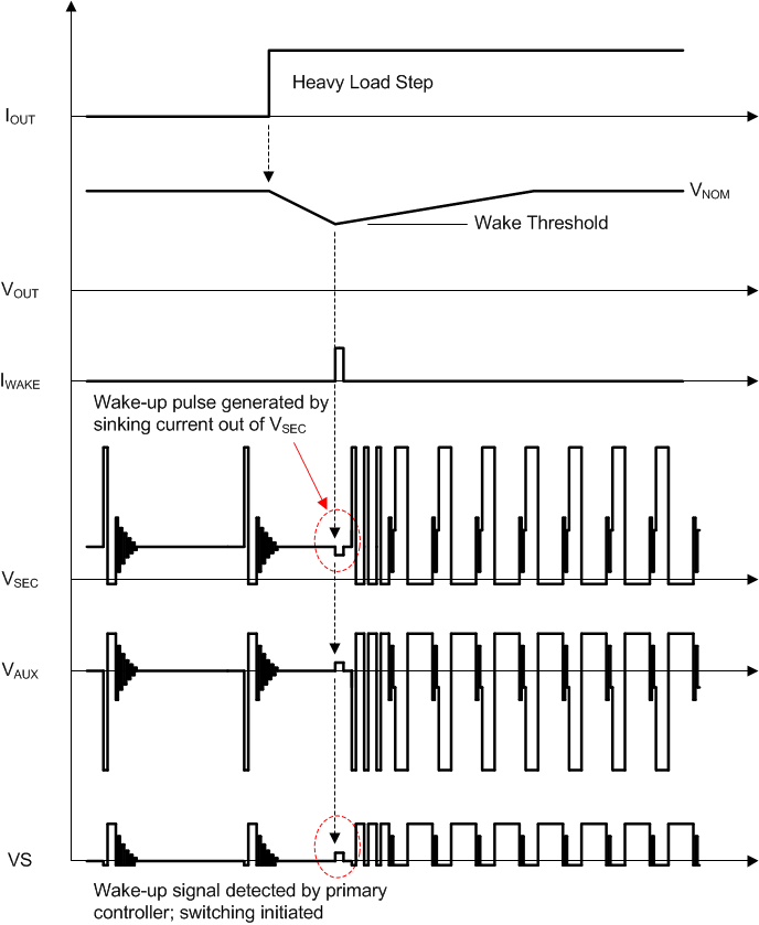
A major feature available at the VS pin is the wake-up function which operates in conjunction with a companion secondary-side wake-up device, such as the UCC24650. This feature allows light-load and no-load switching frequencies to approach 32 Hz to minimize losses, yet wake the UCC28730 from its wait state (sleep mode) in the event of a significant load step between power cycles. Despite the low frequencies, excessive output capacitance is not required to maintain reasonable transient response. While in the wait state, the UCC28730 continually monitors the VS input for a wake-up signal, and when detected, responds immediately with several high-frequency power cycles and resumes operation as required by the control law to recover from the load-step transient and restore output voltage regulation.
Because the wake-up feature interrupts the wait state between very low frequency switching cycles, it allows the use of a much lower output capacitance value than would be required to hold up the voltage without the wake-up function. It also allows the controller to drop to extremely low switching frequencies at no-load conditions to minimize switching losses. This facilitates the achievement of less than 5 mW of input power to meet zero-power stand-by requirements. Use of the UCC28730 controller alone cannot ensure zero-power operation since other system-level limitations are also imposed, however, the UCC28730 and UCC24650 combination goes a long way to reaching this goal.
 Figure 19. Simplified Wake-Up Operation and Waveforms
 The signals illustrated in Figure 19 refer to circuit nodes located on the
Simplified Schematic diagram on the first page of this data sheet. The wake-up signal, which is provided by a secondary-side driver, must meet certain criteria to be considered valid and recognized by the UCC28730 at the VS input. To distinguish the signal from the residual resonant ringing that follows a switching power cycle, the resonant ringing amplitude must diminish and remain below the wake-up signal detection threshold, VWU, for a fixed qualification time, tWUDLY.
The UCC28730 has two such thresholds; one at VWU(low) and one at VWU(high). The lower VWU(low) threshold is used by converters which incorporate a relatively high-impedance driver for the wake-up signal, while the upper VWU(high) threshold may be used in converters with a low-impedance wake-up driver. Both thresholds work exactly the same way. The advantage of the upper threshold is that the UCC28730 is qualified to accept a strong wake-up signal without waiting additional time for the resonant ringing to diminish below the lower threshold.
Figure 20 illustrates the qualification delay period and wake-up response to a low-level wake-up signal. Figure 21 illustrates the qualification delay period and wake-up response to a high-level wake-up signal.
 Figure 20. Wake-Up Qualification Criteria and Wake-Up Response with Low Wake-Up Signal
  Figure 21. Wake-Up Qualification Criteria and Wake-Up Response with High Wake-Up Signal