SLUSC66E March   2015  – February 2017 UCD3138A

PRODUCTION DATA.  

  1. Device Overview
    1. 1.1 Features
    2. 1.2 Applications
    3. 1.3 Description
    4. 1.4 Functional Block Diagram
  2. Device Comparison
    1. 2.1 Product Selection Matrix
  3. Pin Configuration and Functions
    1. 3.1 UCD3138A RGC Package
    2. 3.2 UCD3138A RMH Package
    3. 3.3 UCD3138A RJA Package
  4. Specifications
    1. 4.1 Absolute Maximum Ratings
    2. 4.2 ESD Ratings
    3. 4.3 Recommended Operating Conditions
    4. 4.4 Thermal Information
    5. 4.5 Electrical Characteristics
    6. 4.6 PMBus/SMBus/I2C Timing
    7. 4.7 Peripherals
      1. 4.7.1 Digital Power Peripherals (DPPs)
        1. 4.7.1.1 Front End
        2. 4.7.1.2 DPWM Module
        3. 4.7.1.3 DPWM Events
        4. 4.7.1.4 High Resolution DPWM
        5. 4.7.1.5 Oversampling
        6. 4.7.1.6 DPWM Interrupt Generation
        7. 4.7.1.7 DPWM Interrupt Scaling/Range
        8. 4.7.1.8 DPWM Synchronization
        9. 4.7.1.9 Synchronous Rectifier Dead-Time Optimization Peripheral
    8. 4.8 Typical Temperature Characteristics
  5. Parametric Measurements Information
    1. 5.1 Power-On Reset (POR) and Brown-Out Reset (BOR)
  6. Detailed Description
    1. 6.1 Overview
    2. 6.2 ARM Processor
    3. 6.3 Memory
      1. 6.3.1 CPU Memory Map and interruptions
      2. 6.3.2 Boot ROM
      3. 6.3.3 Customer Boot Program
      4. 6.3.4 Flash Management
    4. 6.4 System Module
      1. 6.4.1 Address Decoder (DEC)
      2. 6.4.2 Memory Management Controller (MMC)
      3. 6.4.3 System Management (SYS)
      4. 6.4.4 Central Interrupt Module (CIM)
    5. 6.5 Feature Description
      1. 6.5.1  Sync FET Ramp and IDE Calculation
      2. 6.5.2  Automatic Mode Switching
        1. 6.5.2.1 Phase Shifted Full Bridge Example
        2. 6.5.2.2 LLC Example
        3. 6.5.2.3 Mechanism for Automatic Mode Switching
      3. 6.5.3  DPWMC, Edge Generation, IntraMux
      4. 6.5.4  Filter
        1. 6.5.4.1 Loop Multiplexer
        2. 6.5.4.2 Fault Multiplexer
      5. 6.5.5  Communication Ports
        1. 6.5.5.1 SCI (UART) Serial Communication Interface
        2. 6.5.5.2 PMBus Interfacte
        3. 6.5.5.3 General Purpose ADC12
        4. 6.5.5.4 Timers
          1. 6.5.5.4.1 24-bit PWM Timer
          2. 6.5.5.4.2 16-Bit PWM Timers
          3. 6.5.5.4.3 Watchdog Timer
      6. 6.5.6  Miscellaneous Analog
      7. 6.5.7  Package ID Information
      8. 6.5.8  Brownout
      9. 6.5.9  Global I/O
      10. 6.5.10 Temperature Sensor Control
      11. 6.5.11 I/O Mux Control
      12. 6.5.12 Current Sharing Control
      13. 6.5.13 Temperature Reference
  7. Device Functional Modes
    1. 7.1 Normal Mode
    2. 7.2 DPWM Multiple Output Mode
    3. 7.3 DPWM Resonant Mode
    4. 7.4 Triangular Mode
    5. 7.5 Leading Edge Mode
  8. Application and Implementation
    1. 8.1 Application Information
    2. 8.2 Typical Application
      1. 8.2.1 Design Requirements
      2. 8.2.2 Detailed Design Procedure
        1. 8.2.2.1 PCMC (Peak Current Mode Control) PSFB (Phase-Shifted Full Bridge) Hardware Configuration Overview
        2. 8.2.2.2 DPWM Initialization for PSFB
      3. 8.2.3 Fixed Signals to Bridge
      4. 8.2.4 Dynamic Signals to Bridge
      5. 8.2.5 System Initialization for PCM
        1. 8.2.5.1 Use of Front Ends and Filters in PSFB
        2. 8.2.5.2 Peak Current Detection
        3. 8.2.5.3 Peak Current Mode (PCM)
      6. 8.2.6 Application Curves
  9. Power Supply Recommendations
    1. 9.1 Power Supply Decoupling and Bulk Capacitors
  10. 10Layout
    1. 10.1 Layout Guidelines
    2. 10.2 Layout Example
  11. 11Device and Documentation Support
    1. 11.1 Device Support
      1. 11.1.1 Development Support
        1. 11.1.1.1 Tools and Documentation
    2. 11.2 Documentation Support
      1. 11.2.1 References
    3. 11.3 Receiving Notification of Documentation Updates
    4. 11.4 Community Resources
    5. 11.5 Trademarks
    6. 11.6 Electrostatic Discharge Caution
    7. 11.7 Glossary
  12. 12Mechanical Packaging and Orderable Information
    1. 12.1 Packaging Information

パッケージ・オプション

メカニカル・データ(パッケージ|ピン)
サーマルパッド・メカニカル・データ
発注情報

Parametric Measurements Information

Power-On Reset (POR) and Brown-Out Reset (BOR)

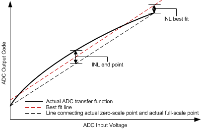
UCD3138A Best_Fit_INL_End_Point_INL_slusc66.gif Figure 5-1 Best Fit INL and End Point INL
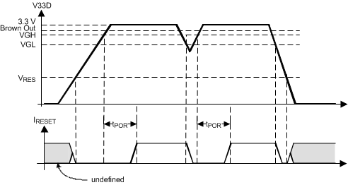
UCD3138A power-on-reset_timing.gif Figure 5-2 Power-On Reset (POR) and Brown-Out Reset (BOR)

Table 5-1 Power-On Reset (POR) and Brown-Out Reset (BOR) Term Definitions

TERM DEFINITION
VGH V33D threshold where the internal power is declared good. The device exits the reset state when above this threshold.
VGL V33D threshold where the internal power is declared bad. The device enters reset state when below this threshold.
Vres V33D threshold where the internal reset signal is no longer valid. Below this threshold the device is in an indeterminate state.
IReset The internal reset signal. When low, the device is held in reset. This is equivalent to holding the device reset pin high.
tPOR The time delay from when the VGH threshold exceeded to when the device exits the reset state.
Brown-out The V33D voltage threshold at which the device sets the brown out status bit. An interrupt can be triggered if enabled.