SLES275A January 2015 – December 2017 VSP5324-Q1
PRODUCTION DATA.
- 1 Features
- 2 Applications
- 3 Description
- 4 Revision History
- 5 Pin Configuration and Functions
-
6 Specifications
- 6.1 Absolute Maximum Ratings
- 6.2 ESD Ratings
- 6.3 Recommended Operating Conditions
- 6.4 Thermal Information
- 6.5 Electrical Characteristics: Dynamic Performance
- 6.6 Electrical Characteristics: General
- 6.7 Electrical Characteristics: Digital
- 6.8 Timing Requirements
- 6.9 LVDS Timing at Different Sampling Frequencies (One-Lane Interface, 12x Serialization)
- 6.10 LVDS Timing at Different Sampling Frequencies (Two-Lane Interface, 6x Serialization)
- 6.11 Serial Interface Timing Requirements
- 6.12 Typical Characteristics
-
7 Detailed Description
- 7.1 Overview
- 7.2 Functional Block Diagrams
- 7.3 Feature Description
- 7.4 Device Functional Modes
- 7.5 Programming
- 7.6
Register Maps
- 7.6.1
Serial Registers
- 7.6.1.1 Register 00h (offset = 00h) [reset = 0]
- 7.6.1.2 Register 01h (offset = 01h) [reset = 0]
- 7.6.1.3 Register 02h (offset = 02h) [reset = 0]
- 7.6.1.4 Register 0Ah (offset = 0Ah) [reset = 0]
- 7.6.1.5 Register 0Fh (offset = 0Fh) [reset = 0]
- 7.6.1.6 Register 14h (offset = 14h) [reset = 0]
- 7.6.1.7 Register 1Ch (offset = 1Ch) [reset = 0]
- 7.6.1.8 Register 23h (offset = 23h) [reset = 0]
- 7.6.1.9 Register 24h (offset = 24h) [reset = 0]
- 7.6.1.10 Register 25h (offset = 25h) [reset = 0]
- 7.6.1.11 Register 26h (offset = 26h) [reset = 0]
- 7.6.1.12 Register 27h (offset = 27h) [reset = 0]
- 7.6.1.13 Register 28h (offset = 28h) [reset = 0]
- 7.6.1.14 Register 29h (offset = 29h) [reset = 0]
- 7.6.1.15 Register 2Ah (offset = 2Ah) [reset = 0]
- 7.6.1.16 Register 2Bh (offset = 2Bh) [reset = 0]
- 7.6.1.17 Register 2Eh (offset = 2Eh) [reset = 0]
- 7.6.1.18 Register 30h (offset = 30h) [reset = 0]
- 7.6.1.19 Register 33h (offset = 33h) [reset = 0]
- 7.6.1.20 Register 35h (offset = 35h) [reset = 0]
- 7.6.1.21 Register 38h (offset = 38h) [reset = 0x0000]
- 7.6.1.22 Register 42h (offset = 42h) [reset = 0]
- 7.6.1.23 Register 45h (offset = 45h) [reset = 0]
- 7.6.1.24 Register 46h (offset = 46h) [reset = 0]
- 7.6.1.25 Register 50h (offset = 50h) [reset = 0]
- 7.6.1.26 Register 51h (offset = 51h) [reset = 0]
- 7.6.1.27 Register 53h (offset = 53h) [reset = 0]
- 7.6.1.28 Register 54h (offset = ) [reset = 0]
- 7.6.1.29 Register 55h (offset = 55h) [reset = 0]
- 7.6.1.30 Register F0h (offset = F0h) [reset = 0]
- 7.6.1
Serial Registers
- 8 Application and Implementation
- 9 Power Supply Recommendations
- 10Layout
- 11Device and Documentation Support
- 12Mechanical, Packaging, and Orderable Information
パッケージ・オプション
メカニカル・データ(パッケージ|ピン)
- RGC|64
サーマルパッド・メカニカル・データ
- RGC|64
発注情報
6 Specifications
6.1 Absolute Maximum Ratings
Over operating free-air temperature range, unless otherwise noted.(1)| MIN | MAX | UNIT | ||
|---|---|---|---|---|
| Supply voltage | AVDD | –0.3 | 2.2 | V |
| LVDD | –0.3 | 2.2 | V | |
| Ground voltage differences | Between AGND and LGND | –0.3 | 0.3 | V |
| Input voltage | Digital outputs | –0.3 | lesser of 2.2 or (LVDD + 0.3) | V |
| Digital inputs (CLKN, CLKP(2), RESET, SCLK, SDATA, CS, SYNC, PD, INT/EXT) | –0.3 | lesser of 2.2 or (LVDD + 0.3) | V | |
| Analog inputs | –0.3 | lesser of 2.2 or (LVDD + 0.3) | V | |
| Input current (all pins except supplies) | –10 | 10 | mA | |
| Ambient temperature, under bias, TA | –40 | 105 | °C | |
| Junction temperature, TJ | 125 | °C | ||
| Storage temperature, Tstg | –55 | 125 | °C | |
(1) Stresses beyond those listed under Absolute Maximum Ratings may cause permanent damage to the device. These are stress ratings only, and do not imply functional operation of the device at these or any other conditions beyond those indicated under Recommended Operating Conditions. Exposure to absolute-maximum-rated conditions for extended periods may affect device reliability.
(2) When AVDD is turned off, TI recommends switching off the input clock (or ensuring the voltage on CLKP, CLKN is less than |0.3 V|). This setting prevents the ESD protection diodes at the clock input pins from turning on.
6.2 ESD Ratings
| VALUE | UNIT | ||||
|---|---|---|---|---|---|
| V(ESD) | Electrostatic discharge | Human body model (HBM), per AEC Q100-002(1) | ±2000 | V | |
| Charged device model (CDM), per AEC Q100-011 | Other pins | ±500 | |||
| Corner pins (1, 16, 17, 32, 33, 48, 49, and 64) | ±750 | ||||
(1) AEC Q100-002 indicates HBM stressing is done in accordance with the ANSI/ESDA/JEDEC JS-001 specification.
6.3 Recommended Operating Conditions
Over operating free-air temperature range, unless otherwise noted.| MIN | NOM | MAX | UNIT | |||
|---|---|---|---|---|---|---|
| V(AVDD) | Analog supply voltage | 1.7 | 1.8 | 1.9 | V | |
| V(LVDD) | Digital supply voltage | 1.7 | 1.8 | 1.9 | V | |
| VID | Differential input voltage | 2 | VPP | |||
| VIC | Input common-mode voltage | VIC ± 50 | mV | |||
| Input clock sample rate | Two-lane LVDS interface | 10 | 80 | MSPS | ||
| One-lane LVDS interface | 10 | 50 | MSPS | |||
| (VCLKP – VCLKM) | Input clock amplitude differential | Sine wave, ac-coupled | 1.5 | VPP | ||
| LVPECL, ac-coupled | 1.6 | VPP | ||||
| LVDS, ac-coupled | 0.7 | VPP | ||||
| LVCMOS, single-ended, ac-coupled | 3.3 | V | ||||
| Duty cycle | 35% | 50% | 65% | |||
| CLOAD | Maximum external capacitance from each output pin to DRGND | 5 | pF | |||
| RLOAD | Differential resistance between LVDS output pairs (LVDS mode) | 100 | Ω | |||
| TA | Operating free-air | –40 | 105 | °C | ||
6.4 Thermal Information
| THERMAL METRIC(1) | VSP5324-Q1 | UNIT | |
|---|---|---|---|
| RGC (VQFN) | |||
| 64 PINS | |||
| RθJA | Junction-to-ambient thermal resistance | 20.6 | °C/W |
| RθJC(top) | Junction-to-case (top) thermal resistance | 6.1 | °C/W |
| RθJB | Junction-to-board thermal resistance | 2.7 | °C/W |
| ψJT | Junction-to-top characterization parameter | 0.2 | °C/W |
| ψJB | Junction-to-board characterization parameter | 2.6 | °C/W |
| RθJC(bot) | Junction-to-case (bottom) thermal resistance | 0.4 | °C/W |
(1) For more information about traditional and new thermal metrics, see the Semiconductor and IC Package Thermal Metrics application report.
6.5 Electrical Characteristics: Dynamic Performance
Typical values are at 25°C, V(AVDD) = 1.8 V, V(LVDD) = 1.8 V, sampling frequency = 80 MSPS, 50% clock duty cycle, and –1-dBFS differential analog input, unless otherwise noted. Minimum and maximum values are across the full temperature range of TMIN = –40°C to TMAX = 105°C, V(AVDD) = 1.8 V, V(LVDD) = 1.8 V.| PARAMETER | TEST CONDITIONS | MIN | TYP | MAX | UNIT | ||
|---|---|---|---|---|---|---|---|
| Resolution | 12 | Bits | |||||
| SNR | Signal-to-noise ratio | ƒIN = 5 MHz | 68 | 70 | dBFS | ||
| ƒIN = 30 MHz | 69.5 | dBFS | |||||
| SINAD | Signal-to-noise and distortion ratio | ƒIN = 5 MHz | 69.8 | dBFS | |||
| ƒIN = 30 MHz | 69.2 | dBFS | |||||
| SFDR | Spurious-free dynamic range | ƒIN = 5 MHz | 64 | 85 | dBc | ||
| ƒIN = 30 MHz | 82 | dBc | |||||
| THD | Total harmonic distortion | ƒIN = 5 MHz | 63 | 81.5 | dBc | ||
| ƒIN = 30 MHz | 78 | dBc | |||||
| HD2 | Second-harmonic distortion | ƒIN = 5 MHz | 64 | 90 | dBc | ||
| ƒIN = 30 MHz | 86 | dBc | |||||
| HD3 | Third-harmonic distortion | ƒIN = 5 MHz | 64 | 85 | dBc | ||
| ƒIN = 30 MHz | 82 | dBc | |||||
| Worst spur (other than second and third harmonics) |
ƒIN = 5 MHz | 91 | dBc | ||||
| ƒIN = 30 MHz | 83 | dBc | |||||
| IMD | Two-tone intermodulation distortion | ƒ1 = 8 MHz, ƒ2 = 10 MHz, each tone at –7 dBFS |
83 | dBc | |||
| Crosstalk (far channel) | 10-MHz full-scale signal on aggressor channel; no input signal applied on victim channel | 95 | dB | ||||
| Input overload recovery | Recovery to within 1% (of full-scale) for 6-dB overload with sine-wave input | 1 | Clock cycle | ||||
| PSRR | AC power-supply rejection ratio | For 50-mVPP signal on AVDD supply, up to 10 MHz, no signal applied to analog inputs |
50 | dB | |||
| ENOB | Effective number of bits | ƒIN = 5 MHz | 11.3 | Bits | |||
| DNL | Differential nonlinearity | ƒIN = 5 MHz | –0.8 | ±0.2 | 0.8 | LSBs | |
| INL | Integral nonlinearity | ƒIN = 5 MHz | ±0.3 | 1 | LSBs | ||
6.6 Electrical Characteristics: General
Typical values are at 25°C, V(AVDD) = 1.8 V, V(LVDD) = 1.8 V, sampling frequency = 80 MSPS, 50% clock duty cycle, and –1-dBFS differential analog input, unless otherwise noted. Minimum and maximum values are across the full temperature range of TMIN = –40°C to TMAX = 105°C, V(AVDD) = 1.8 V, V(LVDD) = 1.8 V.| PARAMETER | TEST CONDITIONS | MIN | TYP | MAX | UNIT | ||
|---|---|---|---|---|---|---|---|
| ANALOG INx_PUT | |||||||
| VID | Differential input | Voltage range | 2 | VPP | |||
| Resistance, at dc | 2 | kΩ | |||||
| Capacitance, at dc | 2.2 | pF | |||||
| Analog input bandwidth | 550 | MHz | |||||
| Analog input common-mode current (per input pin) | 1.6 | µA/ MSPS |
|||||
| VOC | Common-mode output voltage | 0.95 | V | ||||
| IO(VCM) | VCM output current capability | 5 | mA | ||||
| DC ACCURACY | |||||||
| Offset error | ±5 | ±20 | mV | ||||
| EGREF | Gain error resulting from internal reference inaccuracy alone | –2 | 2 | %FS | |||
| EGCHAN | Gain error of channel alone | 0.5 | %FS | ||||
| POWER SUPPLY | |||||||
| IAVDD | Analog supply current | 80 MSPS | 114 | 135 | mA | ||
| 50 MSPS | 86 | mA | |||||
| ILVDD | Output buffer supply current | Two-lane LVDS interface, 80 MSPS, 350-mV swing with 100-Ω external termination | 69 | 85 | mA | ||
| One-lane LVDS interface, 50 MSPS, 350-mV swing with 100-Ω external termination | 56 | mA | |||||
| Analog power | 80 MSPS | 205 | mW | ||||
| 50 MSPS | 155 | mW | |||||
| Digital power LVDS interface | Two-lane LVDS interface, 80 MSPS, 350-mV swing with 100-Ω external termination | 124 | mW | ||||
| One-lane LVDS interface, 50 MSPS, 350-mV swing with 100-Ω external termination | 101 | mW | |||||
| Total power | 80 MSPS, two-lane LVDS interface | 329 | mW | ||||
| 50 MSPS, one-lane LVDS interface | 256 | mW | |||||
| Global power-down | 40 | mW | |||||
| Standby power | 135 | mW | |||||
6.7 Electrical Characteristics: Digital
At V(AVDD) = 1.8 V, V(LVDD) = 1.8 V, unless otherwise noted. The DC specifications refer to the condition where the digital outputs do not switch, but are tied permanently to a valid logic level 0 or 1.| PARAMETER | TEST CONDITIONS | MIN | TYP | MAX | UNIT | ||
|---|---|---|---|---|---|---|---|
| DIGITAL INx_PUTS (RESET, SCLK, SDATA, CS, PDN, SYNC, INT/EXT) | |||||||
| VIH | High-level input voltage | All digital inputs support 1.8-V and 3.3-V CMOS logic levels | > 1.3 | V | |||
| VIL | Low-level input voltage | All digital inputs support 1.8-V and 3.3-V CMOS logic levels | < 0.4 | V | |||
| IIH | High-level input current | VIH = 1.8 V | 6 | µA | |||
| IIL | Low-level input current | VIL = 0 V | < 0.1 | µA | |||
| DIGITAL OUTPUTS | |||||||
| VOH | High-level output voltage | CMOS interface (SDOUT) | AVDD – 0.1 | V | |||
| VOL | Low-level output voltage | CMOS interface (SDOUT) | 0.1 | V | |||
| VOD(H) | High-level output differential voltage | LVDS interface (OUTP, OUTM, LCLKP, LCLKM, ADCLKP, ADCLKM), with an external 100-Ω termination | 245 | 420 | mV | ||
| VOD(L) | Low-level output differential voltage | LVDS interface (OUTP, OUTM, LCLKP, LCLKM, ADCLKP, ADCLKM), with an external 100-Ω termination | –420 | –245 | mV | ||
| VOC | Output common-mode voltage | 1.05 | V | ||||
6.8 Timing Requirements(1)
Typical values are at 25°C, V(AVDD) = 1.8 V, V(LVDD) = 1.8 V, sampling frequency = 80 MSPS, sine wave input clock, C(LOAD) = 5 pF, and R(LOAD) = 100 Ω, unless otherwise noted. Minimum and maximum values are across the full temperature range of TMIN = –40°C to TMAX = 105°C, V(AVDD) = 1.8 V, and V(LVDD) = 1.7 V to 1.9 V.| MIN | NOM | MAX | UNIT | ||||
|---|---|---|---|---|---|---|---|
| Aperture delay | 4 | ns | |||||
| Aperture delay matching(2)(3) | Between the two channels of the same device | ±175 | ps | ||||
| Aperture delay variation | Between two devices at the same temperature and LVDD supply | 2.5 | ns | ||||
| Aperture jitter (RMS) | 320 | fs | |||||
| Wakeup time | Time to valid data after coming out of partial power-down mode |
5 | 50 | µs | |||
| Time to valid data after coming out of global power-down mode |
100 | 500 | µs | ||||
| ADC latency | One-lane LVDS output interface | 11 | Clock cycles | ||||
| Two-lane LVDS output interface | 15 | Clock cycles | |||||
| tsu | Data setup time | Data valid to zero crossing of LCLKP, 80 MSPS, two-lane LVDS |
0.61 | ns | |||
| th | Data hold time(4) | Zero crossing of LCLKP to data becoming invalid, 80 MSPS, two-lane LVDS |
0.74 | ns | |||
| tp | Clock propagation delay | Input clock rising edge crossover to frame clock rising edge crossover, two-lane LVDS for 10 ≤ ƒS ≤ 80 MSPS |
(11 / 12) × tS + td |
ns | |||
| Input clock rising edge crossover to frame clock rising edge crossover, one-lane LVDS for 10 ≤ ƒS ≤ 65 MSPS |
(9 / 12) × tS + td |
ns | |||||
| td | Delay time | 6.8 | 9 | 11.8 | ns | ||
| LVDS bit clock duty cycle | Differential clock duty cycle (LCLKP – LCLKM) | 50 | % | ||||
| tf | Data fall time | Rise time measured from –100 mV to 100 mV, 10 MSPS ≤ sampling frequency ≤ 80 MSPS |
0.2 | ns | |||
| tr | Data rise time | Rise time measured from –100 mV to 100 mV, 10 MSPS ≤ sampling frequency ≤ 80 MSPS |
0.2 | ns | |||
| tr(CLK) | Output clock rise time | Rise time measured from –100 mV to 100 mV, 10 MSPS ≤ sampling frequency ≤ 80 MSPS |
0.18 | ns | |||
| tf(CLK) | Output clock fall time | Rise time measured from –100 mV to 100 mV, 10 MSPS ≤ sampling frequency ≤ 80 MSPS |
0.18 | ns | |||
(1) Timing parameters are ensured by design and characterization and are not tested in production.
(2) C(LOAD) is the effective external single-ended load capacitance between each output pin and ground.
(3) R(LOAD) is the differential load resistance between the LVDS output pair.
(4) Data valid refers to a logic high of 100 mV and a logic low of –100 mV.
6.9 LVDS Timing at Different Sampling Frequencies (One-Lane Interface, 12x Serialization)
See Figure 1 and Figure 2.| MIN | MAX | UNIT | |||
|---|---|---|---|---|---|
| th | LCLKP zero-crossing to data becoming invalid (both edges) | ƒ(SAMPLE) = 40 MSPS | 0.75 | ns | |
| ƒ(SAMPLE) = 50 MSPS | 0.47 | ||||
| ƒ(SAMPLE) = 65 MSPS | 0.25 | ||||
| tsu | Data valid to LCLKP zero-crossing (both edges) | ƒ(SAMPLE) = 40 MSPS | 0.62 | ns | |
| ƒ(SAMPLE) = 50 MSPS | 0.38 | ||||
| ƒ(SAMPLE) = 65 MSPS | 0.19 | ||||
6.10 LVDS Timing at Different Sampling Frequencies (Two-Lane Interface, 6x Serialization)
See Figure 1 and Figure 2.| MIN | MAX | UNIT | |||
|---|---|---|---|---|---|
| th | LCLKP zero-crossing to data becoming invalid (both edges) | ƒ(SAMPLE) = 40 MSPS | 1.9 | ns | |
| ƒ(SAMPLE) = 50 MSPS | 1.55 | ||||
| ƒ(SAMPLE) = 65 MSPS | 1.1 | ||||
| tsu | Data valid to LCLKP zero-crossing (both edges) | ƒ(SAMPLE) = 40 MSPS | 1.44 | ns | |
| ƒ(SAMPLE) = 50 MSPS | 1.02 | ||||
| ƒ(SAMPLE) = 65 MSPS | 0.64 | ||||
6.11 Serial Interface Timing Requirements
See Figure 3.| MIN | MAX | UNIT | ||
|---|---|---|---|---|
| ƒ(SCLK) | SCLK frequency = 1 / tSCLK | > DC | MHz | |
| tsu(LOADS) | SEN to SCLK setup time | 33 | ns | |
| tsu(LOADH) | SCLK to SEN hold time | 33 | ns | |
| tsu(D) | SDATA setup time | 33 | ns | |
| th(D) | SDATA hold time | 33 | ns | |
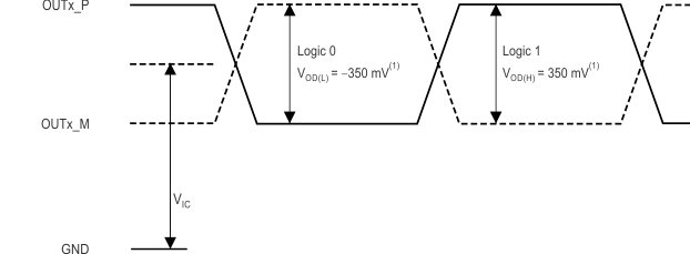
1.
Figure 1. LVDS Output Voltage Levels
NOINDENT:
With an external 100-Ω termination..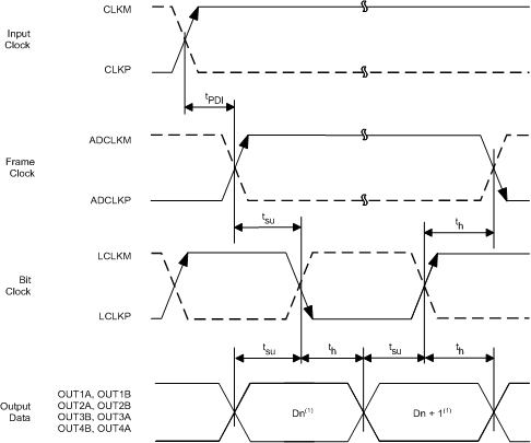 Figure 2. LVDS Mode Timing
 Figure 3. Serial Interface Timing
6.12 Typical Characteristics
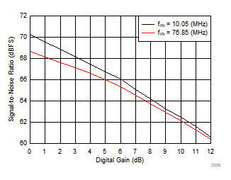
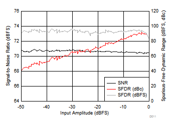
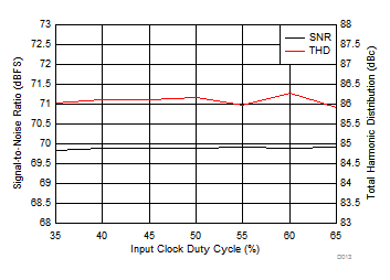
Typical values are at 25°C, V(AVDD) = 1.8 V, V(LVDD) = 1.8 V, 80-MSPS sampling clock frequency, 50% clock duty cycle, and –1-dBFS differential analog input, unless otherwise noted.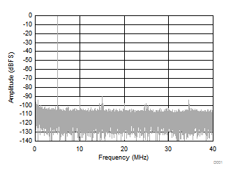
| SNR = 69.6 dBFS | SINAD = 69.5 dBFS |
| SFDR = 89.3 dBc | THD = 85.9 dBc |
| Sample Rate = 80 MSPS |
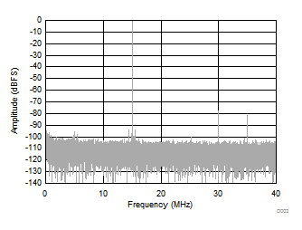
| SNR = 68.5 dBFS | SINAD = 67.8 dBFS |
| SFDR = 76.5 dBc | THD = 75 dBc |
| Sample Rate = 80 MSPS |
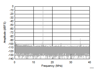
| SNR = 69.6 dBFS | SINAD = 69.4 dBFS |
| SFDR = 84.8 dBc | THD = 83.2 dBc |
| Sample Rate = 80 MSPS |
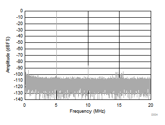
| SNR = 69.8 dBFS | SINAD = 69.7 dBFS |
| SFDR = 85.1 dBc | THD = 84.7 dBc |
| Sample Rate = 40 MSPS |
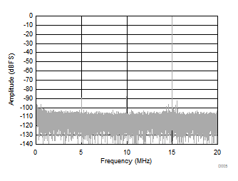
| SNR = 69.6 dBFS | SINAD = 69.5 dBFS |
| SFDR = 86.8 dBc | THD = 84 dBc |
| Sample Rate = 40 MSPS |
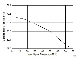
| ƒIN = 5 MHz | ||
| ƒIN = 5 MHz |
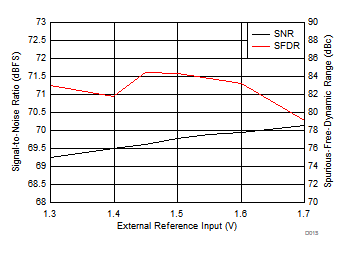
| ƒIN = 5 MHz | External reference using the VCM pin | |
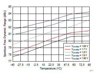
| ƒIN = 5 MHz |
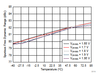
| ƒIN = 5 MHz | ||
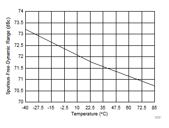
| A 0.7-VPP 5-MHz sine-wave input is applied on the INx_P pin | ||
| The INx_M pin is connected to the device VCM pin |
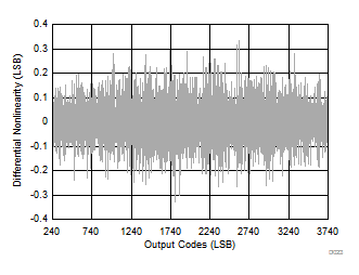
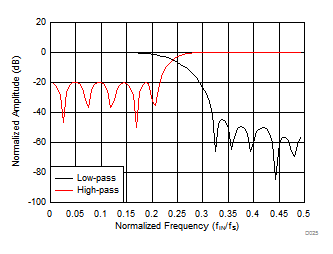 Figure 28. Filter Response (Decimate-by-2)
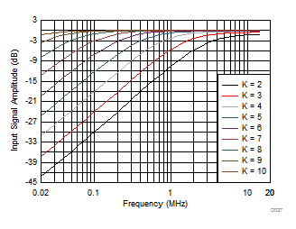
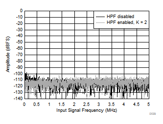
(No Input Signal)
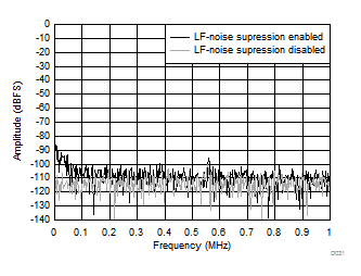 Figure 34. FFT (0 MHz to 1 MHz) for 5-MHz Input Signal
(Sample Rate = 80 MSPS With Low-Frequency Noise Suppression Enabled)
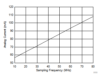 Figure 36. Analog Supply Current
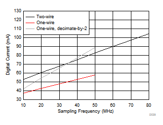 Figure 38. Digital Supply Current
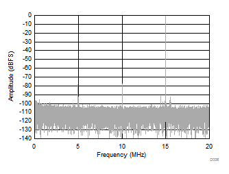
| SNR = 67.2 dBFS | SINAD = 66.6 dBFS |
| SFDR = 76.5 dBc | THD = 74 dBc |
| Sample Rate = 40 MSPS |
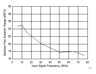
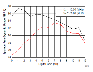
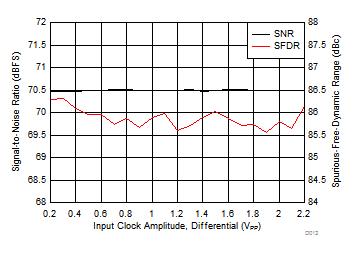
| ƒIN = 5 MHz | ||
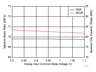
| ƒIN = 5 MHz |
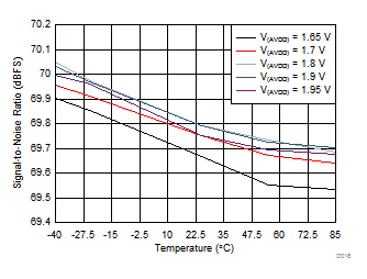
| ƒIN = 5 MHz | ||
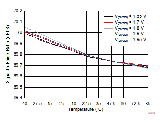
| ƒIN = 5 MHz |
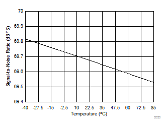
| A 0.7-VPP 5-MHz sine-wave input is applied on the INx_P pin | ||
| The INx_M pin is connected to the device VCM pin |
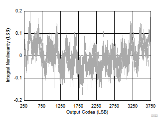
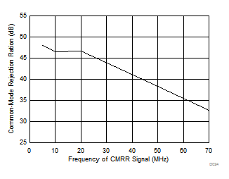
| ƒIN = 3 MHz | 50-mVPP signal superimposed on the input common-mode | |
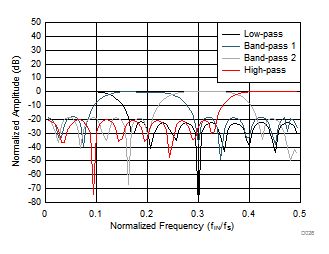 Figure 29. Filter Response (Decimate-by-4)
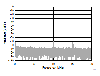
| SNR = 70.8 dBFS | SINAD = 70.7 dBFS | SFDR = 88.7 dBc |
| THD = 87.3 dBc | Decimate-by-2 filter enabled | |
(Sample Rate = 80 MSPS With Decimation Filter = 2)
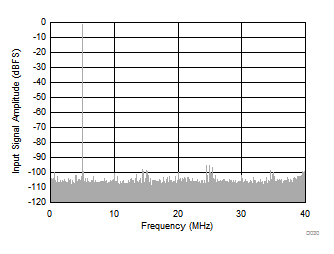
| SNR = 70.8 dBFS | SINAD = 70.7 dBFS |
| SFDR = 88.7 dBc | THD = 87.3 dBc |
(Sample Rate = 80 MSPS With Low-Frequency Noise Suppression Enabled)
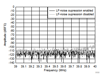 Figure 35. FFT (39 MHz to 40 MHz) for 5-MHz Input Signal
(Sample Rate = 80 MSPS With Low-Frequency Noise Suppression Enabled)
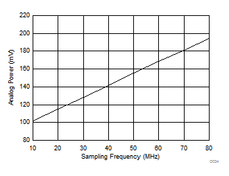 Figure 37. Power Consumption on Analog Supply
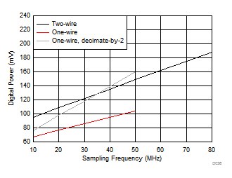 Figure 39. Power Consumption on Digital Supply