JAJSC56F December   2012  – March 2018 UCC27611

PRODUCTION DATA.  

  1. 特長
  2. アプリケーション
  3. 概要
    1.     Device Images
      1.      代表的なアプリケーションの図
  4. 改訂履歴
  5. Pin Configuration and Functions
    1.     Pin Functions
  6. Specifications
    1. 6.1 Absolute Maximum Ratings
    2. 6.2 ESD Ratings
    3. 6.3 Recommended Operating Conditions
    4. 6.4 Thermal Information
    5. 6.5 Electrical Characteristics
    6. 6.6 Switching Characteristics
    7. 6.7 Typical Characteristics
  7. Detailed Description
    1. 7.1 Overview
    2. 7.2 Functional Block Diagram
    3. 7.3 Feature Description
      1. 7.3.1 VDD and Undervoltage Lockout
      2. 7.3.2 Operating Supply Current
      3. 7.3.3 Input Stage
      4. 7.3.4 Enable Function
      5. 7.3.5 Output Stage
      6. 7.3.6 Low Propagation Delays
    4. 7.4 Device Functional Modes
  8. Application and Implementation
    1. 8.1 Application Information
    2. 8.2 Typical Application
      1. 8.2.1 Design Requirements
      2. 8.2.2 Detailed Design Procedure
        1. 8.2.2.1 Gate Drive Supply Voltage
        2. 8.2.2.2 Input Configuration
        3. 8.2.2.3 Output Configuration
        4. 8.2.2.4 Power Dissipation
        5. 8.2.2.5 Thermal Considerations
      3. 8.2.3 Application Curves
  9. Power Supply Recommendations
  10. 10Layout
    1. 10.1 Layout Guidelines
    2. 10.2 Layout Example
  11. 11デバイスおよびドキュメントのサポート
    1. 11.1 ドキュメントのサポート
      1. 11.1.1 関連資料
    2. 11.2 ドキュメントの更新通知を受け取る方法
    3. 11.3 コミュニティ・リソース
    4. 11.4 商標
    5. 11.5 静電気放電に関する注意事項
    6. 11.6 Glossary
  12. 12メカニカル、パッケージ、および注文情報

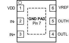
Pin Configuration and Functions

DRV Package
6-Pin SON With Exposed Thermal Pad
Top View
UCC27611 pin_lusba5.gif

Pin Functions

PIN I/O DESCRIPTION
NO. NAME
1 VDD I Bias supply input. Connect a ceramic capacitor minimum from this pin to the GND pin as close as possible to the device with the shortest trace lengths possible.
2 IN– I Inverting input. Pull IN+ to VDD to enable output, when using the driver device in Inverting configuration.
3 IN+ I Noninverting input. Pull IN– to GND to enable output, when using the driver device in noninverting configuration.
4 OUTL O 6-A sink current output of driver.
5 OUTH O 4-A source current output of driver.
6 VREF O Drive voltage, output of internal linear regulator. Connect a ceramic capacitor minimum from this pin to the GND pin as close as possible to the device with the shortest trace lengths possible.
7 GND PAD Ground. All signals are referenced to this node.