JAJSE92B November 2017 – April 2018 TPSM84824
PRODUCTION DATA.
- 1 特長
- 2 アプリケーション
- 3 概要
- 4 改訂履歴
- 5 Pin Configuration and Functions
- 6 Specifications
-
7 Detailed Description
- 7.1 Overview
- 7.2 Functional Block Diagram
- 7.3
Feature Description
- 7.3.1 Adjusting the Output Voltage
- 7.3.2 Switching Frequency (RT)
- 7.3.3 Synchronization (CLK)
- 7.3.4 Output On/Off Enable (EN)
- 7.3.5 Input Capacitor Selection
- 7.3.6 Output Capacitor Selection
- 7.3.7 TurboTrans (TT)
- 7.3.8 Undervoltage Lockout (UVLO)
- 7.3.9 Soft Start (SS/TR)
- 7.3.10 Sequencing (SS/TR)
- 7.3.11 Power Good (PGOOD)
- 7.3.12 Safe Start-up into Pre-Biased Outputs
- 7.3.13 Overcurrent Protection
- 7.3.14 Thermal Shutdown
- 7.4 Device Functional Modes
- 8 Application and Implementation
- 9 Power Supply Recommendations
- 10Layout
- 11デバイスおよびドキュメントのサポート
- 12メカニカル、パッケージ、および注文情報
7.3.1 Adjusting the Output Voltage
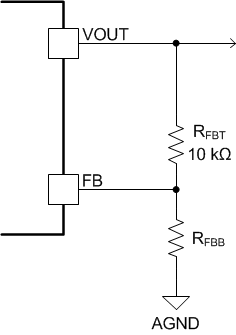
A resistor divider connected to the FB pin (pin 2) programs the output voltage of the TPSM84824. The output voltage adjustment range is from 0.6 V to 10 V. Figure 12 shows the feedback resistor connection for setting the output voltage. The recommended value of RFBT is 10 kΩ. The value for RFBB can be calculated using Equation 1 or simply selected from the range of values given in Table 1. Table 1 also includes the recommended switching frequency and minimum required output capacitance for each output voltage.
Equation 1. 

 Figure 12. Setting the Output Voltage
Table 1. Standard Component Values
| VOUT (V) | RFBB (kΩ) | RECOMMENDED
fSW (kHz) |
RRT (kΩ) | Minimum Required COUT(µF)(1)(2) | |
|---|---|---|---|---|---|
| CERAMIC | POLYMER(3) | ||||
| 0.6 | open | 250 | 200 | 400 | 220 |
| 0.7 | 60.4 | 250 | 200 | 400 | 220 |
| 0.8 | 30.1 | 300 | 165 | 300 | 220 |
| 0.9 | 20.0 | 350 | 143 | 200 | 220 |
| 1.0 | 15.0 | 400 | 124 | 200 | - |
| 1.1 | 12.1 | 400 | 124 | 200 | - |
| 1.2 | 10.0 | 450 | 110 | 200 | - |
| 1.3 | 8.66 | 500 | 97.6 | 200 | - |
| 1.4 | 7.50 | 500 | 97.6 | 200 | - |
| 1.5 | 6.65 | 550 | 88.7 | 150 | - |
| 1.6 | 6.04 | 550 | 88.7 | 150 | - |
| 1.7 | 5.49 | 600 | 82.5 | 150 | - |
| 1.8 | 4.99 | 600 | 82.5 | 100 | - |
| 1.9 | 4.64 | 650 | 75.0 | 100 | - |
| 2.0 | 4.32 | 700 | 69.8 | 100 | - |
| 2.5 | 3.16 | 800 | 60.4 | 100 | - |
| 3.3 | 2.21 | 1000 | 48.7 | 47 | - |
| 5.0 | 1.37 | 1200 | 40.2 | 47 | - |
| 6.0 | 1.10 | 1200 | 40.2 | 47 | - |
| 7.5 | 0.866 | 1300 | 36.5 | 47 | - |
| 9.0 | 0.715 | 1300 | 36.5 | 22 | - |
| 10 | 0.634 | 1300 | 36.5 | 22 | - |
(1) Additional capacitance above the minimum can be ceramic or polymer type.
(2) Load transients with > 2 A/µs slew rates or load steps exceeding 4 A may require additional capacitance, see TurboTrans.
(3) See Low-ESR Output Capacitors for details on polymer capacitors.