JAJSF78L June 2006 – May 2018 TPS65023 , TPS65023B
PRODUCTION DATA.
- 1 特長
- 2 アプリケーション
- 3 概要
- 4 改訂履歴
- 5 概要(続き)
- 6 Pin Configuration and Functions
-
7 Specifications
- 7.1 Absolute Maximum Ratings
- 7.2 ESD Ratings
- 7.3 Recommended Operating Conditions
- 7.4 Thermal Information
- 7.5 Electrical Characteristics
- 7.6 Electrical Characteristics: Supply Pins VCC, VINDCDC1, VINDCDC2, VINDCDC3
- 7.7 Electrical Characteristics: Supply Pins VBACKUP, VSYSIN, VRTC, VINLDO
- 7.8 Electrical Characteristics: VDCDC1 Step-Down Converter
- 7.9 Electrical Characteristics: VDCDC2 Step-Down Converter
- 7.10 Electrical Characteristics: VDCDC3 Step-Down Converter
- 7.11 I2C Timing Requirements for TPS65023B
- 7.12 Typical Characteristics
-
8 Detailed Description
- 8.1 Overview
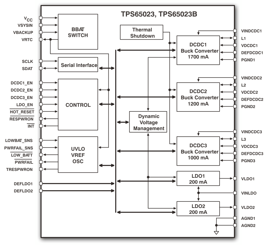
- 8.2 Functional Block Diagram
- 8.3
Feature Description
- 8.3.1 VRTC Output and Operation With or Without Backup Battery
- 8.3.2 Step-Down Converters, VDCDC1, VDCDC2, and VDCDC3
- 8.3.3 Power Save Mode Operation
- 8.3.4 Low Ripple Mode
- 8.3.5 Soft-Start
- 8.3.6 100% Duty Cycle Low Dropout Operation
- 8.3.7 Active Discharge When Disabled
- 8.3.8 Power-Good Monitoring
- 8.3.9 Low-Dropout Voltage Regulators
- 8.3.10 Undervoltage Lockout
- 8.3.11 Power-Up Sequencing
- 8.4 Device Functional Modes
- 8.5 Programming
- 8.6
Register Maps
- 8.6.1 VERSION Register Address: 00h (Read Only)
- 8.6.2 PGOODZ Register Address: 01h (Read Only)
- 8.6.3 MASK Register Address: 02h (Read and Write), Default Value: C0h
- 8.6.4 REG_CTRL Register Address: 03h (Read and Write), Default Value: FFh
- 8.6.5 CON_CTRL Register Address: 04h (Read and Write), Default Value: B1h
- 8.6.6 CON_CTRL2 Register Address: 05h (Read and Write), Default Value: 40h
- 8.6.7 DEFCORE Register Address: 06h (Read and Write), Default Value: 14h/1Eh
- 8.6.8 DEFSLEW Register Address: 07h (Read and Write), Default Value: 06h
- 8.6.9 LDO_CTRL Register Address: 08h (Read and Write), Default Value: Set with DEFLDO1 and DEFLDO2
- 9 Application and Implementation
- 10Power Supply Recommendations
- 11Layout
- 12デバイスおよびドキュメントのサポート
- 13メカニカル、パッケージ、および注文情報
