JAJSF78L June 2006 – May 2018 TPS65023 , TPS65023B
PRODUCTION DATA.
- 1 特長
- 2 アプリケーション
- 3 概要
- 4 改訂履歴
- 5 概要(続き)
- 6 Pin Configuration and Functions
-
7 Specifications
- 7.1 Absolute Maximum Ratings
- 7.2 ESD Ratings
- 7.3 Recommended Operating Conditions
- 7.4 Thermal Information
- 7.5 Electrical Characteristics
- 7.6 Electrical Characteristics: Supply Pins VCC, VINDCDC1, VINDCDC2, VINDCDC3
- 7.7 Electrical Characteristics: Supply Pins VBACKUP, VSYSIN, VRTC, VINLDO
- 7.8 Electrical Characteristics: VDCDC1 Step-Down Converter
- 7.9 Electrical Characteristics: VDCDC2 Step-Down Converter
- 7.10 Electrical Characteristics: VDCDC3 Step-Down Converter
- 7.11 I2C Timing Requirements for TPS65023B
- 7.12 Typical Characteristics
-
8 Detailed Description
- 8.1 Overview
- 8.2 Functional Block Diagram
- 8.3
Feature Description
- 8.3.1 VRTC Output and Operation With or Without Backup Battery
- 8.3.2 Step-Down Converters, VDCDC1, VDCDC2, and VDCDC3
- 8.3.3 Power Save Mode Operation
- 8.3.4 Low Ripple Mode
- 8.3.5 Soft-Start
- 8.3.6 100% Duty Cycle Low Dropout Operation
- 8.3.7 Active Discharge When Disabled
- 8.3.8 Power-Good Monitoring
- 8.3.9 Low-Dropout Voltage Regulators
- 8.3.10 Undervoltage Lockout
- 8.3.11 Power-Up Sequencing
- 8.4 Device Functional Modes
- 8.5 Programming
- 8.6
Register Maps
- 8.6.1 VERSION Register Address: 00h (Read Only)
- 8.6.2 PGOODZ Register Address: 01h (Read Only)
- 8.6.3 MASK Register Address: 02h (Read and Write), Default Value: C0h
- 8.6.4 REG_CTRL Register Address: 03h (Read and Write), Default Value: FFh
- 8.6.5 CON_CTRL Register Address: 04h (Read and Write), Default Value: B1h
- 8.6.6 CON_CTRL2 Register Address: 05h (Read and Write), Default Value: 40h
- 8.6.7 DEFCORE Register Address: 06h (Read and Write), Default Value: 14h/1Eh
- 8.6.8 DEFSLEW Register Address: 07h (Read and Write), Default Value: 06h
- 8.6.9 LDO_CTRL Register Address: 08h (Read and Write), Default Value: Set with DEFLDO1 and DEFLDO2
- 9 Application and Implementation
- 10Power Supply Recommendations
- 11Layout
- 12デバイスおよびドキュメントのサポート
- 13メカニカル、パッケージ、および注文情報
9.2.2.4 Output Voltage Selection
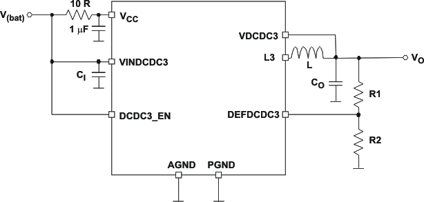
The DEFDCDC1, DEFDCDC2, and DEFDCDC3 pins are used to set the output voltage for each step-down converter. See Table 20 for the default voltages if the pins are pulled to GND or to VCC. If a different voltage is needed, an external resistor divider can be added to the DEFDCDCx pin as shown in Figure 41.
The output voltage of VDCDC1 is set with the I2C interface. If the voltage is changed from the default, using the DEFCORE register, the output voltage only depends on the register value. Any resistor divider at DEFDCDC1 does not change the voltage set with the register.
Table 20. DCDC1, DCDC2, and DCDC3 Default Voltage Levels
| PIN | LEVEL | DEFAULT OUTPUT VOLTAGE |
|---|---|---|
| DEFDCDC1 | VCC | 1.6 V |
| GND | 1.2 V | |
| DEFDCDC2 | VCC | 3.3 V |
| GND | 1.8 V | |
| DEFDCDC3 | VCC | 3.3 V |
| GND | 1.8 V |
Using an external resistor divider at DEFDCDCx:
 Figure 41. External Resistor Divider
 When a resistor divider is connected to DEFDCDCx, the output voltage can be set from 0.6 V up to the input voltage V(bat). The total resistance (R1 + R2) of the voltage divider must be kept in the 1-MR range to maintain a high efficiency at light load.
V(DEFDCDCx) = 0.6 V
